
Opamp Circuits Loaded Noninverting Amplifier - PowerPoint PPT Presentation
1 / 46
Title:
Opamp Circuits Loaded Noninverting Amplifier
Description:
The base current of the second BJT is the load current, divided by the second BJT's beta: ... and with a beta equal to the product of the individual betas. ... – PowerPoint PPT presentation
Number of Views:381
Avg rating:3.0/5.0
Title: Opamp Circuits Loaded Noninverting Amplifier
1
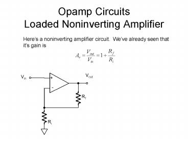
Opamp CircuitsLoaded Noninverting Amplifier
Heres a noninverting amplifier circuit. Weve
already seen that its gain is
Vout
Vin.
-
Rf
Ri
2
Opamp CircuitsLoaded Noninverting Amplifier
Now, suppose we connect a load resistor RL to the
opamps output
Vout
Vin.
-
RL
Rf
Ri
3
Opamp CircuitsLoaded Noninverting Amplifier
If the opamp is trulyan ideal opamp, Eout is
always equal to Vout, and the load resistor does
not effect Vout.
Vin.
Vout
Eout
-
-
RL
Rf
Ri
4
Opamp CircuitsLoaded Noninverting Amplifier
If the opamp is a real-world opamp, like an LM741
or LM324, its output current Iout is limited to
some maximum value. As long as Iout is less than
the opamps output current rating, the opamp
behaves like an ideal opamp. With no load
resistor, Iout If. With the load resistor
connected, Iout If Iloadt.
Vout
Iout
Iload
Vin.
Since Rf and Ri are effectively in series,
-
RL
Rf
If
Ri
5
Opamp CircuitsLoaded Noninverting Amplifier
If and Iload will both be largest when Vout is
driven to the upper rail. Lets assume the
supply Voltages are 15 V and -15 V, and Vout can
go all the way to the rails (zero headroom).
Lets also assume that Rf 10 KW and Ri 1 KW,
and the maximum output current for this opamp is
10 mA. Under these conditions,
Vout
Iout
Iload
Vin.
-
This does not exceed the opamps maximum output
current, so without the load resistor the circuit
works properly.
RL
Rf
If
Ri
6
Opamp CircuitsLoaded Noninverting Amplifier
Now, lets connect an 11 KW load resistor (RL
11 KW). Now load current is drawn
The total output current is the sum of the load
current and If, so
Vout
Iout
Iload
Vin.
-
RL
Rf
If
Which is still less than the opamps maximum
output current.
Ri
7
Opamp CircuitsLoaded Noninverting Amplifier
Lets load the opamp more heavily. This means
reducing the value of the load resistor to, say,
1100 W.
Now the load current alone is enough to overload
the opamps output stage, so the circuit will not
work unless an opamp with a higher output current
rating is used.
Vout
Iout
Iload
Vin.
-
RL
Rf
If
Ri
8
Opamp CircuitsLoaded Noninverting Amplifier
The total output current for this circuit is
so to drive an 1100 W load, we should choose an
opamp with an output current rating of at least
15 mA.
Vout
Iout
Iload
Vin.
-
RL
Rf
If
Ri
9
Opamp CircuitsNoninverting Amplifier with BJT
Current Boost
15 V
Heres a way to use an opamp with a relatively
low maximum output current to drive a load which
exceeds the opamps drive capability. An
external BJT is used to drive the load. The BJT
is controlled by the opamp. Notice
Vin.
-
-15 V
that the BJT is inside the feedback loop. This
makes it, in effect, part of the opamp output
stage.
Rf
Vout
Vfb.
RL
Ri
10
Opamp CircuitsNoninverting Amplifier with BJT
Current Boost
As we saw before, Vfb is derived from Vout by the
Voltage divider consisiting of Rf and Ri
15 V
The ideal opamp assumptions still dictate that V
V-, so
b 50
Vin.
-
-15 V
Rf
Vout
Vfb.
RL
Ri
11
Opamp CircuitsNoninverting Amplifier with BJT
Current Boost
As we saw with the simple loaded noninverting
amplifier,
15 V
Vin.
b 50
-
Iout
If Ri 1 KW, Rf 10 KW, and RL 100 W, then
Iout is 151 mA. Without the current booster,
this would overload an opamp rated at 10 mA, or
even 50 or 100 mA.
IL
-15 V
Rf
Vout
Vfb.
RL
If
Ri
12
Opamp CircuitsNoninverting Amplifier with BJT
Current Boost
But with the BJT current booster, the BJT acts as
the source of Iout. The opamp only has to source
15 V
Vin.
b 50
For the given element values, Ri 1 KW, Rf 10
KW, and RL 100 W, Ib 3.02 mA. An opamp with
10 mA of output drive capability would be plenty.
-
Iout
Ib
IL
-15 V
Rf
Vout
Vfb.
RL
If
Ri
13
Opamp CircuitsNoninverting Amplifier with BJT
Current Boost
How is the output Voltage affected by the
addition of the BJT? If the opamps output were
capable of going all the way to the positive
supply rail (zero headroom), the Voltage at the
load terminal (Vout) would be the 15 V supply
Voltage reduced by the
15 V
Vin.
b 50
BJTs 0.7 V base-emitter Voltage drop. The
maximum output Voltage would be 14.3 V, so the
headroom requirement would be increased by 0.7 V.
-
Iout
Ib
IL
-15 V
Rf
Vout
Vfb.
RL
If
Ri
14
Opamp CircuitsNoninverting Amplifier with
MOSFET Current Boost
Its also possible to use a MOSFET to boost the
current drive capability of an opamp. A
MOSFETs gate terminal is insulated from the
source, drain and bulk, so ideally no current
flows in the gate. In the real world, the gate
has very high (but not infinite) leakage
resistance, so a very
15 V
Vin.
small gate current must be sourced by the opamp.
This is a much smaller current than was the case
with the BJT current booster. See Example 9-17
in the textbook.
-
Iout
IL
-15 V
Rf
Vout
Vfb.
RL
If
Ri
15
Opamp CircuitsNoninverting Amplifier with
Active Feedback
15 V
Heres a current-boosted opamp with a second
opamp in the feedback path. This is called
active feedback.
Vin.
b 50
-
The second opamp is connected as a noninverting
amplifier, with Vsense as its input Voltage and
Vfb as its output, so
Ib
Vout
15 V
-15 V
RL
Vfb.
Vsense
Rsense
Rf
Ri
16
Opamp CircuitsNoninverting Amplifier with
Active Feedback
15 V
RL and Rsense are essentially in series, so they
form a Voltage divider
Vin.
b 50
-
Ib
Vout
15 V
-15 V
Combining this relationship with the previous one
yields this
RL
Vfb.
Vsense
Rsense
Rf
Ri
17
Opamp CircuitsNoninverting Amplifier with
Active Feedback
15 V
Once again, the ideal opamp assumptions dictate
that Vin Vfb, so
Vin.
b 50
-
Ib
Vout
15 V
-15 V
Which we solve for Vout
RL
Vfb.
Vsense
Rsense
Rf
Ri
18
Opamp CircuitsNoninverting Amplifier with
Active Feedback
15 V
In the textbooks example, Vin 4 V, Rf 1.1
KW, Ri 10 KW, RL 2 W, and Rsense 0.1 W.
Vin.
b1 100
-
b 30
Ib
Vout
15 V
-15 V
RL
Vfb.
Vsense
The load current is
Rsense
Rf
Ri
19
Opamp CircuitsNoninverting Amplifier with
Active Feedback
15 V
The base current of the second BJT is the load
current, divided by the second BJTs beta
Vin.
b1 100
-
b 30
Ib
Vout
15 V
-15 V
The output current of the feedforward opamp is
the base current of the first BJT
RL
Vfb.
Vsense
Rsense
Rf
Ri
20
Opamp CircuitsNoninverting Amplifier with
Active Feedback
15 V
There are two base-emitter Voltage drops between
the output of the feedforward opamp and Vout, so
the
Vin.
b1 100
headroom is reduced by at least 1.4 V (2x 0.7 V),
possibly a bit more since power transistors
sometimes exhibit a greater VBE. Note The two
BJTs are connected so they behave like a single
BJT, but with a base-emitter Voltage drop equal
to the sum of the individual VBEs, and with a
beta equal to the product of the individual
betas. This is called a darlington-connected
pair.
-
b 30
Ib
Vout
15 V
-15 V
RL
Vfb.
Vsense
Rsense
Rf
Ri
21
Opamp CircuitsInverting Amplifier Summing
Amplifier
Heres an inverting amplifier. As noted before,
V- V because of the ideal opamp assumptions,
so V- 0 V. This means the current flowing
through R1 is
The ideal opamp assumptions also say no current
may flow into either of the opamps inputs, so
all of I1 must flow through Rf. The Voltage drop
across Rf is I1Rf, and one end of it is connected
to a virtual ground (V-), so the end thats
connected to the
Rf
opamps output is at the potential given by
Esupply
V1.
R1
V-.
-
LM324
I1.
Vout
-Esupply
22
Opamp CircuitsInverting Amplifier Summing
Amplifier
Heres the same amplifier, with the addition of a
second input Voltage V2, and a second input
resistor R2. The new input current is
Its still true that no current may flow into
either of the opamps inputs, so all of I1 and I2
must flow through Rf. Now the Voltage drop
across Rf is (I1 I2)Rf, so
Rf
R2
V2.
I2.
Esupply
V1.
R1
V-.
-
LM324
I1.
Vout
-Esupply
23
Opamp CircuitsInverting Amplifier Summing
Amplifier
Weve made something called a weighted summer.
It sums the two input Voltages V1 and V2, after
first multiplying each by a constant (or weight)
k1 and k2, respectively.
Rf
R2
V2.
I2.
Esupply
V1.
R1
V-.
-
LM324
I1.
Vout
-Esupply
24
Opamp CircuitsInverting Amplifier Summing
Amplifier
We could add as many additional inputs and input
resistors as we like, within reason, to sum
additional terms
Rj
Vj.
Rf
R2
V2.
I2.
Esupply
V1.
R1
V-.
-
LM324
I1.
Vout
-Esupply
25
Opamp CircuitsZero and Span Amplifier
Heres an LM34 temperature sensor, a device which
has no input, only an output Voltage (VT, below)
which is proportional to temperature. For the
LM34, VT 0 at 0 degrees F, and increases 10 mV
for every degree of temperature increase. At 32
degrees F, VT 320 mV. At 212 degrees F, VT
2.120 V.
Esupply
VT
26
Opamp CircuitsZero and Span Amplifier
Wed like to build a circuit which develops an
output Voltage which gives the temperature in
degrees Celsius. At 0 degrees C (32 degrees F),
Vout 0 V at 100 degrees C (212 degrees F),
Vout 1.00 V. The LM34s output Voltage is 320
mV at 0 degrees C (because that temperature is
also 32 degrees F), so the first step is to
cancel that 320 mV by subtracting an equal amount.
Esupply
Farenheit to Celsius Conversion
Vout
VT
27
Opamp CircuitsZero and Span Amplifier
This is done with a two-input summing amplifier,
as shown below. If R1 and R2 have the same
value,
R2
-320 mV.
At 0 degrees F, VT 320 mV, so V1 0. If
we choose Rf so k 1, then Vout will be -1.8 V
at 100 deg. C (212 deg. F), but we want it to be
1.00 V at that temperature.
Rf
Esupply
I2.
R1
V-.
-
VT
Vout
28
Opamp CircuitsZero and Span Amplifier
The next thing to do is to choose Rf and R1 so
the gain of the amplifier is
If Rf 1.0 kW and Rf 1.8 kW, k 1/1.8. Now,
at 0 deg. C, V2 0 V, and at 100 deg. C, V2
-1.00 V. The only thing left to do is add a
unity-gain inverter to make V2 1.00 V at 100
deg. C.
R2 1.8 kW
-320 mV.
Rf 1.0 kW
Esupply
I2.
R1
V-.
-
1.8 kW
VT
V2
29
Opamp CircuitsZero and Span Amplifier
Heres the complete zero and span amplifier, so
named because it permits the designer to choose
the input Voltage (VT here) which results in an
output of zero, and it also allows the designer
to choose the output
Voltage range spanned by a given input Voltage
range.
R2 1.8 kW
-320 mV.
Rf 1.0 kW
10 kW
Esupply
I2.
R1
10 kW
-
1.8 kW
-
VT
V2
Vout
30
Opamp CircuitsDifference Amplifier
Now our bag of tricks includes the following
31
Opamp CircuitsDifference Amplifier
Wed like to add a circuit whose output is
proportional to the difference between two input
Voltages V1 and V2. The circuit below does that
Its a difference amplifer. Notice that R1 and
R2 form a Voltage divider, so
The ideal opamp assumptions dictate that V- V,
so
Rf
I1
V1.
Ri
-
I1
Vout
V2.
R1
R2
32
Opamp CircuitsDifference Amplifier
The ideal opamp assumptions also say that the
current flowing through Rf is equal to I1,
because the ideal opamp has infinite input
resistance. The Voltage drop across Rf is I1 Rf.
The output Voltage is
Rf
I1
V1.
Ri
-
I1
Vout
V2.
R1
R2
33
Opamp CircuitsDifference Amplifier
If we choose the resistance values so that
then
Rf
I1
V1.
Ri
-
I1
Vout
V2.
R1
R2
34
Opamp CircuitsDifference Amplifier
Suppose R1 Ri 1000 W, R2 Rf 100 kW
Rf
I1
V1.
Ri
-
I1
Vout
V2.
R1
R2
35
Opamp CircuitsDifference Amplifier
What is the input resistance of the difference
amplifier? The resistance which would be
measured at V1 given by
Rf
I1
V1.
Ri
-
I1
Vout
V2.
R1
R2
36
Opamp CircuitsDifference Amplifier
The resistance at input V1 is
Which is a function of both V1 and V2. Thats
not good it would be much better if the input
resistance were constant.
Rf
I1
V1.
Ri
Also, the gain of the difference amplifier is
given by
-
I1
Vout
V2.
R1
R2
So changing or adjusting the circuit gain
requires changing or adjusting the values of two
resistors. One would be much better.
37
Opamp CircuitsInstrumentation Amplifier
These drawbacks can be overcome by using the
instrumentation amplifier circuit below. Both
inputs are applied directly to the noninverting
inputs, so the input resistances are equal to the
input resistance of the opamp constant, and
ideally infinite.
Vin
Vout
-
I1
Vin-
Ri2
Rf2
I1
-
I3
I3 I2
I2 I1
Rf1
Ri1
Rg
I1
I2
38
Opamp CircuitsInstrumentation Amplifier
Examination of the circuit and use of the ideal
opamp assumptions tell us that
Vin
Vout
-
I1
Vin-
Ri2
Rf2
I1
-
I3
I3 I2
I2 I1
Rf1
Ri1
Rg
I1
I2
39
Opamp CircuitsInstrumentation Amplifier
Combining the five expressions yields this
Vin
Vout
-
I1
Vin-
Ri2
Rf2
I1
-
I3
I3 I2
I2 I1
Rf1
Ri1
Rg
I1
I2
40
Opamp CircuitsInstrumentation Amplifier
Grouping the Vin terms together, and the Vin-
terms together
Vin
Vout
-
I1
Vin-
Ri2
Rf2
I1
-
I3
I3 I2
I2 I1
Rf1
Ri1
Rg
I1
I2
41
Opamp CircuitsInstrumentation Amplifier
Vin
Vout
-
I1
If Rf1, Rf2, Ri1 and Ri2 are chosen so that
Vin-
Ri2
Rf2
I1
-
I3
I3 I2
I2 I1
Rf1
Ri1
Rg
The following is the result
I1
I2
42
Opamp CircuitsInstrumentation Amplifier
Vin
Vout
-
I1
Vin-
Ri2
Rf2
I1
-
I3
I3 I2
I2 I1
Rf1
Ri1
Adm is the differential mode gain of the
instrumentation amplifier circuit
Rg
I1
I2
43
Opamp CircuitsInstrumentation Amplifier
The first two terms determine a minimum gain,
which does not depend on Rg. The last term is
the variable gain term, which can be controlled
by adjusting the value of Rg.
Vin
Vout
-
I1
Vin-
Ri2
Rf2
I1
-
I3
I3 I2
I2 I1
Rf1
Ri1
Rg
I1
I2
44
Opamp CircuitsCurrent to Voltage Converter
Heres a circuit which converts a current input
to a Voltage output. The ratio of output Voltage
to input current has units of Volts/Amperes, or
Ohms, which is the unit of resistance. This
circuit can also be called a transresistance
(short for transfer resistance) amplifier
Vout
-
Rf
Iin
Notice that Iin flows into a virtual ground. If
Iin is supplied by an ideal current source (or
something that approximates an ideal current
source) then the current is independent of
Voltage.
45
Opamp Circuits Voltage to Current Converter
Heres a circuit which converts a Voltage input
to a current output. The ratio of output current
to input Voltage has units of Amperes/Volts, or
Siemens, which is the unit of conductance. This
circuit can also be called a transconductance
(short for transfer conductance) amplifier
Vin
-
Iout
Rload
Rf
46
Opamp Circuits Active Diode
Heres a circuit which makes
Iload
Vin
Vout
-
10 kW
Rload
Recommended
CrystalGraphics Presentations


