
nanoTX USA 08: Accelerating Nanotechnology Commercialization - PowerPoint PPT Presentation
1 / 27
Title:
nanoTX USA 08: Accelerating Nanotechnology Commercialization
Description:
Modern evolutionary theory teaches us: ... Open intelligent networks. Light bulbs. and Nanotechnology ... I need to improve my golf game or tennis score. This ... – PowerPoint PPT presentation
Number of Views:61
Avg rating:3.0/5.0
Title: nanoTX USA 08: Accelerating Nanotechnology Commercialization
1
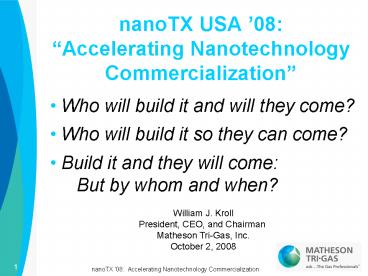
nanoTX USA 08Accelerating Nanotechnology
Commercialization
- Who will build it and will they come?
- Who will build it so they can come?
- Build it and they will come
- But by whom and when?
William J. Kroll President, CEO, and Chairman
Matheson Tri-Gas, Inc. October 2, 2008
2
(No Transcript)
3
Outline
- Nanotechnology is new but is following a business
pattern. - Limits are being seen in the education skill base
to support this. - Technology problems that are being addressed by
nanotechnology are there. - Where are the centers for cooperative development
in this area? - Here is the model we are using.
4
Semiconductor Technology, A Convergence of
Technology and Business Models By Dr. Bernard S.
Meyerson, IBM Fellow, VP Strategic Alliances and
CTO
5
Semiconductor Technology, A Convergence of
Technology and Business Models By Dr. Bernard S.
Meyerson, IBM Fellow, VP Strategic Alliances and
CTO
6
- Nanotechnology
- Evolution
- Revolution
- or just plain good old Business?
7
Modern evolutionary theory teaches us
- Evolution proceeds via both small large
innovations (mutations). - Over long periods of time, there are vastly more
small innovations than large ones. - Over long periods of time, the distribution of
innovation "size" conforms to a power-law
distribution. - Over short periods of time, evolution may be seen
to be either gradual (dominated by many small
innovations) or revolutionary (dominated by major
innovations). - Major innovations tend to spur bursts of minor
innovations. - Over time, the accumulation of a large number of
minor innovations lays the foundation for later
major innovations.
8
Phrases sound familiar?
- It has been used for
- Automobiles
- Cell phones
- Rational databases
- Open intelligent networks
- Light bulbs
- and Nanotechnology
9
Perception versus Reality
- Nano applications been in use for a long time
- Old Paintings
- Stained glass windows
- London Fog
- Commercial applications in coatings, inkjets, and
electronics started over 40 years ago - It is already impacting the way we live
10
So Why the Hype?
- Risk, Benefit Analysis
- Replaces dot com as the new business venture
- I need to improve my golf game or tennis score
- This generation is getting older
- Need the drugs
- Lighter tools, phones, furniture
- Applications, benefits, and economics impact are
becoming evident
11
Roadblocks to Nanotechnology
- Ultimately, nanotechnology is still suffering
with the so-called - roadblocks to the market. The primary challenge
nowadays - is to recognize commercial applications of
research and to fill - in the vocabulary gap of nanotechnology
ignorance. - Therefore, future roadblocks to successful
application of may be - Recognizing commercial application of research
- Implementation of high volume manufacturing of
nanotechnology - High costs of nano materials
- Lack of interaction between science and market
- Lack of qualified professional staff for
research at universities - Handling, transportation of nanotechnology
material - Availability of instrumentation
- What is further interesting to note, is the
opposition nanotechnology - has received from traditional media outlets that
talk about the - potential negative consequences of nanotechnology
such as - Crichtons Prey.
12
SIA Workforce Strategy Overview, David R. Ferrell
13
Nanotechnology its not just for breakfast
anymore! What are we missing?
SIA Workforce Strategy Overview, David R. Ferrell
14
If you can solve the education problem, you
dont have to do anything else. If you dont
solve it, nothing else is going to matter all
that much. - Alan Greenspan, former
Federal Reserve Board chairman
15
If you can solve the education problem, you
dont have to do anything else. If you dont
solve it, nothing else is going to matter all
that much. - Alan Greenspan, former
Federal Reserve Board chairman
CRS Report for Congress, Foreign Science
Engineering Presence in U.S. Institutions and the
Labor Force (7/23/08)
16
Why things dont scale (Myerson IBM)
- Moores Law requires smaller transistors to be
made, - where each dimension of that transistor is
reduced - generation after generation
- Some layers in transistors are now only 5-6 atoms
thick, and can no longer be correctly scaled - The failure of proper scaling results in
transistors producing far more heat than can be
tolerated - New materials and processes must thus be invented
at each new technology node to enable continued
progress in semiconductor technology
17
Semiconductor Technology, A Convergence of
Technology and Business Models By Dr.
Bernard S. Meyerson, IBM Fellow, VP
Strategic Alliances and CTO
18
Next Generation Switch
Semiconductor Technology, A Convergence of
Technology and Business Models By Dr. Bernard S.
Meyerson, IBM Fellow, VP Strategic Alliances and
CTO
19
(No Transcript)
20
Semiconductor Technology, A Convergence of
Technology and Business Models By Dr. Bernard S.
Meyerson, IBM Fellow, VP Strategic Alliances and
CTO
21
From IBM/NEC release IBM's other joint dev.
partners include Chartered, Freescale,Infineon,
Samsung,STMicroelectronics Toshiba
9/10/08 IBM NEC announced joint Development
at Albany NanoTech
22
Drivers
- Perhaps we should view Moores Law as innovation
driver for - Directed assembly, which may enable extensibility
of affordable CMOS fabrication to 10 nm - Enhanced patterning functions, beyond masking,
such as 3D nanofabrication and deterministic
placement of electronically useful nanostructures - Materials-by-design, including engineered
interfaces and the heterogeneous materials
integration on CMOS - Predictive nanomaterials models, which
concurrently optimize nanomaterial performance
and ESH impact
We need materials options that circumvent Moores
Law
23
Nanopillars
24
NSF NNI Long-term View for Nanotechnology RD
(Mike Roco, NSF-NNI)
- From "From Vision to Reality The NNI at Five
Years - by Mihail " Mike" Roco (2006)
- http//www.nanohub.org/resources/1230/
- Today, nanotechnology is expanding at the global
level and on an - accelerating path
- from passive nanostructured components to active
nanosystems - from scientific discovery to technological
innovation - in areas such advanced materials, electronics,
and pharmaceutical - to new areas of relevance such as biomedical,
energy, environment, - agriculture food systems, and controlled
molecular architectures - for manufacturing
- For this reason, it is essential to
- have a robust RD program
- select most suitable investments
- anticipate possible scenarios
- address societal aspects from the beginning of
large RD investments.
25
Nanophotonic
- YORKTOWN HEIGHTS, NY - 17 Mar 2008
- IBM (NYSE IBM) scientists today took another
significant advance towards sending - information inside a computer chip by using light
pulses instead of electrons by - building the worlds tiniest nanophotonic switch
with a footprint about 100X smaller - than the cross section of a human hair.
- The switch is an important building block to
control the flow of information inside future
chips and can significantly speed up the chip
performance while using much less energy. - Todays announcement is a continuation of a
series of IBM developments towards an on-chip
optical network - In November 2005, IBM scientists demonstrated a
silicon nanophotonic device that can
significantly slow down and actively control the
speed of light. - In December 2006, an analogous tiny silicon
device was used to demonstrate buffering of over
a byte of information encoded in optical pulses a
requirement for building optical buffers for
on-chip optical networks. - In December 2007, IBM scientists announced the
development of an ultra-compact silicon
electro-optic modulator, which performs the job
of converting electrical signals into the light
pulses, a prerequisite for enabling on-chip
optical communications.
26
Innovation is Evolving
- Seeing a lot of talk but looking for the walk
- It makes business sense
- When your investors ask when are they going to
see a return in the market place - The answer should be you already are
- Innovation is a food chain
- Is Innovation on an internal basis creating the
value?
27
Matheson Tri-Gas Technology Vision
Do not seek to follow in the footsteps of the
wise. Seek what they sought. Basho We
recognize that our path is different from our
traditional competitors, and that this
difference is our strength. We see ourselves as
a flexible responsive supplier of unique
products and technology that will give our
customers the competitive edge they need in order
to thrive.
Recommended
CrystalGraphics Presentations


