
Overview of Nanofabrication - PowerPoint PPT Presentation
1 / 73
Title:
Overview of Nanofabrication
Description:
Overview of Nanofabrication Material depostion methods Thin films of materials Thickness measurement Lithography Pattern transformation on to planar suface – PowerPoint PPT presentation
Number of Views:666
Avg rating:3.0/5.0
Title: Overview of Nanofabrication
1
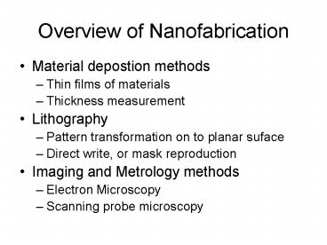
Overview of Nanofabrication
- Material depostion methods
- Thin films of materials
- Thickness measurement
- Lithography
- Pattern transformation on to planar suface
- Direct write, or mask reproduction
- Imaging and Metrology methods
- Electron Microscopy
- Scanning probe microscopy
2
Thin film deposition techniques
- Vacuum deposition Methods
- UHV (lt10-8), HV
- Sputtering
- CVD
- Laser Oblation
- Thermal deposition
- Boat or crucible, E-gun
- Epitaxy, growth models
3
Sputtering
substrate
Target material
B
E
Ar
Vacuum 10-3 Torr Ar
- RF plasma rectifies RF power, gives DC
acceleration voltage - Ions circle B field lines, increase colisson
probability
Ar, N2
RF Power
4
E-beam evaporator
5
E-gun
Filament
6
Thermal CVD system
Precurser Gas For growing Carbon Nanotubes
http//www.iljinnanotech.co.kr/en/material/r-4-4.h
tm
7
Carbon Nanotubes
http//www.iljinnanotech.co.kr/en/material/r-4-4.h
tm
8
MBE
"Molecular Beam Epitaxy is a versatile technique for growing thin epitaxial structures made of semiconductors, metals or insulators." In a ultra-high vacuum, a beam of atoms or, more general, a beam of molecules is directed towards a crystalline substrate such that the atoms or molecules stick at the substrates surface forming a new layer of deposited material. But where is the difference between MBE and other material deposition methods as e.g. thermal vacuum evaporation?
http//www.wsi.tu-muenchen.de/E24/resources/facili
ties.htm
9
MBE and surface analysis chamber
10
The Knudsen Cell (effusion cell)
http//www.grc.nasa.gov/WWW/RT2002/5000/5160coplan
d.html
11
Lithography
- Spin coat radiation sensitive polymer - Resist
- Expose layer (through mask or direct write)
- Develop
- Etch away or deposit material
12
Positive and negative resist
13
Liftoff requires undercut
14
Resist Contrast Curve
Logarithmic measure of slope of contrast curve
Negative Resist
Positive Resist
100
Film Retention
0
D2
D1
15
Positive Resist Chemistry
16
Molecular weight shift
17
Typical Positive Resist process
- EXAMPLE PROCESS AZ5206 POSITIVE MASK PLATE
- Soak mask plate in acetone gt 10 min to remove the
original photoresist. - Rinse in isopropanol, blow dry.
- Clean the plate with RIE in oxygen. Do not use a
barrel etcher. - RIE conditions 30 sccm O2, 30 mTorr total
pressure, 90 W (0.25 W/cm2), 5 min. - Immediately spin AZ5206, 3 krpm.
- Bake at 80 C for 30 min.
- Expose with e-beam, 10 kV, 6 C/cm2, Make sure the
plate is well grounded. - (Other accelerating voltages may be used, but
the dose will be different.) - Develop for 60 s in KLK PPD 401 developer. Rinse
in water. - Descum - important Same as step 2 above, for only
5 seconds - Or use a barrel etcher, 0.6 Torr oxygen,
150W, 1 min. - If this is a Cr plate, etch with Transene Cr
etchant, 1.5 min. - If this is a MoSi plate, then RIE etch
- 0.05 Torr total pressure, 0.05 W/cm2, 16
sccm SF6, 4.2 sccm CF4,1 min. - Plasma clean to remove resist same as step 2
above, for 3 min.
18
Negative Resist Cemistry
19
Typical Negative resist process
- EXAMPLE PROCESS SAL NEGATIVE MASK PLATE
- Soak mask plate in acetone gt 10 min to remove
photoresist. - Clean the plate with RIE in oxygen. Do not use a
barrel etcher. - RIE conditions 30 sccm O2, 30 mTorr total
pressure, 90 W (0.25 W/cm2), 5 min. - Immediately spin SAL-601, 4 krpm, 1 min.
- Bake in 90 C oven for 10 min. This resist is not
sensitive to room light. - Expose at 50 kV, 11 C/cm2. Be sure the plate is
grounded. - Post-bake for 1 min on a large hotplate, 115 C.
- Cool for gt 6 min.
- Develop for 6 min in Shipley MF312water (11) Be
sure to check for underdevelopment. - Descum 30 s with oxygen RIE same as step 2, 10
s. - Etch with Transene or Cyantek Cr etchant, 1.5
min. - Plasma clean to remove resist Same as step 2, 5
min.
20
Photo Lithography
- Project UV light through Mask
- Non contact with optical reduction (typical 4X)
- Contact with one-to-one pattern transfer
- Mask very flat SiO2 plate with Cr thin film
- Resolution limited by wave length (phase shift)
- Optics hard for short wave lengths
21
Electron Beam Lithograpy
- Literature, Resources
- Handbook of Microlithography Micromachining and
Microfabrication, ed. P. Rai-Choudhury, SPEI
press (chapter two is on the web, linked from
home page - J C Nabity web site http//www.jcnabity.com
- Course material is posted on web site in
restricted area - http//www.nanophys.kth.se ? education ?
Intro. to e-beam Lithography - Link to restricted area (password protected)
- Username ebeamlecture
- Password lithogr
22
Some things you can do with EBL
Circuit of SQUIDs and Josephson Tunnel Junctions
23
1.5 mm
Bonding Pads
Contact cage to nano-circuit -- for rapid
testing
24
Connecting Strips
25
Ferromagnetic - Normal metal tunnel junctions
Co
100 nm
Al
Circuit to measure spin injection from
ferromagnet (Co) to normal metal (Al)
26
Innerdigitated Capacitor in coplanar waveguide
Cooper Pair Transistor
27
- All these structure were made with
- one layer of e-beam lithography and one vacuum
deposition cycle!
28
Block Diagram on an EBL system
29
Electron Optics
detector
sample
Scanning the electron beam
30
Beam diameter
31
Electron scattering limits resolution
Higher energy electrons have larger
back-scattering range
32
Double Gaussian profile
33
Overview of systems
- SEM conversion (NPGS)
- SEM modification (Raith)
- High end system
- SEM conversion limited in speed by slow beam
deflection system (induction in magnet coils). - Laser stage is big step in price, but necessary
for accurate pattern writing and stitching. - The more complex the system, the more service and
higher user costs - Industry Fab. machines not always well suited to
research needs.
34
NPGS
- Joe Nabity, one man company, good reputation,
very helpful, good support - Works with many SEMS
- Can do stage control, many SEMs come with
micrometer, motor control (accuracy) - Can do precision alignment in single field by
scanning in reduced area to find mark. Manual
mark detection.
Good Web site http//www.jcnabity.com list
of references, pictures, ideas
35
Fabricated with NPGS
This image shows a pattern of radially placed
dots in PMMA after development. The white bar at
the bottom of the image is 1 micron long. The
pattern was designed as radial lines, but the
spacing of the exposure points was set 0.3
microns to produce discrete dots. Notice how the
dot size and spacing is very consistent in all
directions. The exposure was done with an SEM
with no beam blanker and the image was taken with
the NPGS digital imaging feature. The pattern was
written by Dr. ChiiDong Chen at the Institute of
Physics, Academia Sinica, Taiwan.
This picture shows part of a circular grating
with a period of 0.15 microns. The lines appear
almost straight, because they are near the outer
edge of the grating where the radius is 100
microns. The pattern was written in PMMA and has
been coated with gold for viewing. The
lithography was done at the Optical Sciences
Center at the University of Arizona.
36
Raith 150(KTH and Lund in Sweden)
- Expanding company, niche for mid range system
- Based on conversion of Zeiss FE Sem, high quality
SEM, good detector - Also sell conversion system (Elphay Quantum)
- Control system has bugs, poor software support
- Software has good features simple cad, position
list, direct exposure control - Laser stage not perfect, but accurate overlay and
stitching has been achieved - Can take a 6 inch (150mm) wafer
37
Proven resolution with our Raith 150 courtesy of
Anders Holmberg
LLine width (pitch 2L)
38
High End system, designed for Industry Fab.
39
Nanophys positive process for one-cycle tunnel
junction fabrication
- Two layer resist, selective developers
- Very large undercut suspended bridge
- Tunnel junction (top and base layer) in one layer
Top view of pattern
Exposed areas
Undercut region
Supporting resist
Next slides Cut on this axis
40
Lithography and shadow evaporation
ZEP 520
PMGI SF7
SiOx
Si
41
Lithography and shadow evaporation
Irradiate with electron beam
42
Lithography and shadow evaporation
Develop the two layers selectively Top layer
Bottom Layer
43
Lithography and shadow evaporation
Evaporate Al at an angle
44
Lithography and shadow evaporation
Oxidize the first layer
45
Lithography and shadow evaporation
Evaporate Al at opposite angle
46
Lithography and shadow evaporation
Lift off the resist and excess metal
Tunnel junctions
47
Voilà
Circuit of SQUIDs and Josephson Tunnel Junctions
48
3D structuring using contrast curve
- Accurately measure thickness of film
- Do test pattern with dose profile to accurately
measure contrast curve
49
Patterning in third dimension
Desired structure
thickness
Dose
50
Holography
Positive electron resist SAL 110 Developer SAL
101 (Shipley)
Chalmers Group, S. Hård et al. Applied Optics
vol. 33 p 1176, 1994
51
Optical Kinoforms
Chalmers Group, S. Hård et al. Applied Optics
vol. 33 p 1176, 1994 Optical Comm. Vol. 88, p 37,
1992
52
Two basic types of pattern methods
- Direct Writing
- Change pattern with each run
- Slow, serial method of fabrication
- Good for research and development
- Low through-put, too costly for large scale
production - Lithography
- pattern copying one process step
- Fast, parallel method
- High through-put makes low cost in large scale
prod. - Not flexible enough for research and development.
53
Comparison of Lithographic methods
- Photo Lithography
- UV, deep UV
- Projection or contact
- Micro contact printing
- Stamp formed from Soft material
- Molecules (ink) is wet on to stamp, transferred
to surface - Printing Press
54
Micro Contact printing
http//www.research.philips.com/technologies/light
_dev_microsys/softlitho/
55
Stamp fabrication
- Master made by direct writing methods (EBL on Si
etch) - Stamp gets dirty, wears out
- Essentially old-style printing methods scaled to
nm dimensions
56
SAMs and molecular electronics
57
Optical Stepper
http//www.sematech.org
http//www.nanonet.go.jp/
58
For example Nikon optical steppers
59
High through-put direct writing tool
Sigma 700 series from Micronic Laser systems,
Täby Sweden
http//www.micronic.se
Spatial Light Modulator (SLM) chip 10 6
electronically addressable mirrors
60
Alignment and overlay
- Alignment and overlay are more serious problems
than actually making the small structure! - Large area with fine detail requires stitching
write fields together laser interferometer
stage, nm position and metrological accuracy! - Overlay requires accurate alignment marks, mark
detection, registration and extremely accurate
pattern placement over large area (scaling
accuracy 1 part 106).
61
3-layer process done in Albanova
Industry has MUCH more sophisticated circuits
with 15-20 layers, 108 components, with very
accurate overlay
62
Metrology and Imaging
- Laser interferometers on Stage
- 5nm resolution
- Reproducibility
- Thickness measurement
- Profilometer, demonstration
- Scanning Probe microscipe
- Vertrical resolution 1 Å level
- Latteral resolution depends on tip sharpness
63
SPM system overview
64
Scanning Tunneling Microscopy (STM)Binnig and
Rohrer 1981 (Nobel Prize in Physics 1986)
Electric current proportional to
quantum mechanical probablility amplitude of
tunneling through the energy barrier
Wavefunction decays eponentially in barrier
region
65
Single Atom imaging possible
- Sharp tip
- Pristine surface
- Ultra High Vacuum
The making of a Quanum Corral Fe atoms on a Cu
(111) surface
Check out this web page
http//www.almaden.ibm.com/vis/stm/gallery.html
66
Atomic Force Microscopy (AFM)
Two Basic AFM Modes Contact mode (no vibrating
tip) Tapping mode (vibrating tip) Many
variations on Scanning Force Microscopy Liquid
AFM Magnetic Force Microscopy (MFM) Latteral
Force Microscopy (LFM) Intermitant and
non-contact AFM Force Modulation Microscopy
(FMM) Electrostatic Force Microscopy (EFM)
67
Atomic Forces
Hard core repulsion Contact region
Force
z Seperation between tip and surface
Attractive force van der Walls Non-contact retion
68
Image molecular monolayers in liquid
- Molecules must be immobilized on surface
- Local force measurements possible
S-layer protein monolayer on Si surface in liquid
environment, 500 nm x 500 nm Zentrum für
Ultrastrukturforschung - Universität für
Bodenkultur. Austria
69
Two basic scanning modes
- Feedback off Scan over surface with constant z0
(piezo voltage), control signal changes with
tip-surface separation. - Feedback on circuit regulates z piezo voltage
to constant value of control signal (constantly
changes tip-surface separation).
70
AFMContact mode
71
AFM tapping mode
Free space oscillation of cantilever resonance
10-100 kHz
Cantilever hits surface smaller amplitude of
oscillation
72
Feedback loop tapping mode
Free oscillation Large amplitude
Hitting surface lower amplitude
73
Digital Insturments Multi-Mode head, scanner and
base
- Turn on the controller (the computer should be
left on) - Remove the scanner from under the microscope.