
Task VI: Predictive Modeling and Metrology Predictive Process, Property, Performance Models - PowerPoint PPT Presentation
1 / 1
Title:
Task VI: Predictive Modeling and Metrology Predictive Process, Property, Performance Models
Description:
Properties. Spatial variation - processes. Thin-film-specific effects. Thermo-mechanical stress ... Can associate spatially varying properties with grains. ... – PowerPoint PPT presentation
Number of Views:188
Avg rating:3.0/5.0
Title: Task VI: Predictive Modeling and Metrology Predictive Process, Property, Performance Models
1
Task VI Predictive Modeling and
MetrologyPredictive Process, Property,
Performance Models
SEMICONDUCTOR SUPPLIERS
M. O. Bloomfield, S. Sen, J. Zhang, Y. H. Im, V.
Prasad, D. Datta, M. S. Shephard, and T. S. Cale
Focus Center - New York
www.cieem.rpi.edu/fc-ny
Virtual Prototyping via Predictive Process,
Property, Performance Modeling
Modeling and Simulation Objective
- Driver Relationships
- Multiscale microstructure modeling for predictive
simulation tool development. - By the end of 2002 we will be done with the
initial results of this phase of the work. We
expect to have a continued broad response to our
successes. - Structural and property predictions to be coupled
with performance models. Forming teams to start
these efforts in Q302. - Atomistic and molecular modeling team
- Property prediction team
- Materials and process models can be used to
assess process flows and materials sets. - Continuing to integrate microstructure tools with
equipment models.
- Predictive Processing Property Performance Models
- Focus on 3D nanoscale polycrystalline films
- Replace correlations and empirical guidelines
with predictive models - Materials models
- Process Models
- P4 modeling and simulation is a long term vision
- Structure as a function of Processing
- Effects of structure on properties and
performance - Help synthesize the disparate/fragmented global
efforts to predict interconnect relevant
microstructure evolution.
- Tools
- Atomistic/energetic/pathway models
- Microstructure models
- Multiscale process, materials and performance
models
- Predict performance from
- Materials properties
- Process conditions
- Operating environment
- Performance
- Thin film performance
- Failure analysis / lifetime
- Assess process flows
- Identify trouble spots
- Circuit performance
- Properties
- Spatial variation - processes
- Thin-film-specific effects
- Thermo-mechanical stress
- Diffusion through multilayers
- Adhesion
- Structure
- Texture (grain orientation)
- Grain sizes
- Interface morphology (e.g., roughness) and
composition - Defect distributions (interface and bulk)
5-8 yrs
3-5 yrs
3-7 yrs
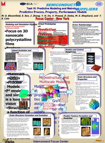
Predict and Control Roughness
Island Evolution and Growth
- Goal Develop models to assist optimization of
roughness-sensitive structures e.g., optical
waveguides and vertical cavity lasers. - Use 3D/2D simulations
- to understand origins of roughening
- to evaluate transport and reaction models
- to control/minimize roughening
- Trends of RIE simulations (top left figure) agree
with polymer etch experiments done at RPI - Smoother surfaces (decreased interface
thicknesses) at higher pressures (radical/ion
ratio up). RMS roughness becomes constant at
long times for high pressures, but increases
linearly with material removed at low pressures. - Very slight correlation length increase with etch
depth.
- Goal Predict microstructure formation during
thin film nucleation and growth. - Discrete to continuum conversion at reasonable
island sizes. - Measured or simulated nucleation data can be used
to determine starting structure for 3D island
evolution. - 3D surface and microstructure evolution code
(FEBLE).
Using atomic layer deposition to alleviate
roughening
Quantum dots (Oktyabrsky)
Nucleation data (Yang, Cale)
AFM image of rough polymer surface etched using
RIE.
Agarwal et al.
KLMC simulations - texture competition (Huang,
Gilmer)
Continuum Islands
(Agarwal et al.).
Gria
Microstructure and Multiscale Modeling Grand
Challenge Grain-Continuum Modeling
Predict Stressesin Multilayers
Grain Structure and Properties
Goal Develop modeling tools that predict
stresses in multilayer stacks, with film
thicknesses lt 100 nm e.g., for 3-D interconnect
systems.
- Goal Develop models and tools for the
determination of grain structure evolution and
properties. - Model 3D grain structure evolution using a finite
element based level set solver. - Develop meshes to obtain 3D descriptions of grain
structure and associated transport volume. - Currently using a tetrahedral volume mesh with
approx. 250,000 elements and 46,000 nodes to
describe single grain. Mesh generator used is QMG
2.0 developed at Cornell. - Generated meshes can be used for solving
Boltzmann or diffusive transport problems and for
Material properties assigned separately to each
grain
- Use ANSYS to evaluate the stresses caused by
thermal expansion mismatch between copper and
silicon. Conservative assumptions lead us to
predict no Si failure due to 380o C cycle.
Can recover the discrete nature of model as needed
- Thicker barrier layers result in slightly reduced
stresses. - Introduction of intentional void in via results
in reduced stresses. - Presence of multiple vias in a periodic
arrangement may reduce tensile stress in silicon. - Extend analysis to study transient thermal
stresses during processing to study coupled
thermal and mechanical effects. - Combine dislocation theory with grain-continuum
film model to predict stress and strain behavior
in thin films (lt100 nm thick). - Couple with adhesion and grain evolution models
to predict overall mechanical behavior in 3-D
multilayer interconnect systems.
- field solution.
- Generated meshes can also be used for
stress-strain analysis, analysis of
electromigration and defect densities.
Grainboundaries
P4 tools will allow processes and material sets
to be evaluated in a Virtual Wafer Fab
3D tetrahedral volume mesh of a single grain.
Grain Structure Formation and Evolution
Predict Texture Formation and Evolution
- Finite Element-Based Levelset Evolver (FEBLE)
uses levelsets on locally refineable meshes to
track islands as they evolve and interact. Can
associate spatially varying properties with
grains. - Uses multiple levelsets to robustly handle
topography and geometry changes, and to
facilitate physical calculations, e.g.,
curvature driven grain boundary motion. - Parallel code that can take advantage of many
processors, distributed environments. - Connecting several process models e.g., ECD,
ELD, PVD, CVD, solidification, and ALD. - Can take input from, track geometry changes for
other evolution models, e.g., ripening, twin
growth, grain rotation.
- Goal Develop models that predict texture
formation and evolution in polycrystalline films.
Interface with property and performance models. - Use results of multiple-lattice atomistic (KLMC)
models for texture formation during deposition
and evolution during processing and operation. - Grain-continuum modeling will track texture and
other microstructural properties. - Validate models using experimental measurements.
c90
c
c0
Coalesced grain structure
Initial, nucleated substrate
Experimental data (Lu et al.)
Single, meshed grain
Bottom view
FEBLE simulation
Kinetically controlled, electroless deposition
onto a substrate with 5 nm rms roughness.
Interconnect Focus Center
Recommended
CrystalGraphics Presentations


