
The Analog Sampler history in SACLAY - PowerPoint PPT Presentation
1 / 14
Title:
The Analog Sampler history in SACLAY
Description:
simultaneous W/R sampler N ADC clocked with a common Fs/N clock. ... No high frequency clock. No problem of huge power dissipation of a single chip ... – PowerPoint PPT presentation
Number of Views:51
Avg rating:3.0/5.0
Title: The Analog Sampler history in SACLAY
1
The Analog Sampler history in SACLAY
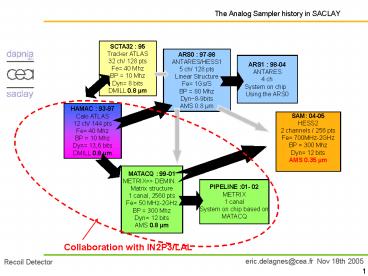
SCTA32 95 Tracker ATLAS 32 ch/ 128 pts Fe 40
Mhz BP 10 Mhz Dyn 8 bits DMILL 0.8 µm
ARS0 97-98 ANTARES/HESS1 5 ch/ 128 pts Linear
Structure Fe 1Gs/S BP 80 Mhz Dyn8-9bits AMS
0.8 µm
ARS1 98-04 ANTARES 4 ch System on chip Using
the ARS0
HAMAC 93-97 Calo ATLAS 12 ch/ 144 pts Fe 40
Mhz BP 10 Mhz Dyn 13,6 bits DMILL 0.8 µm
SAM 04-05 HESS2 2 channels / 256 pts Fe
700MHz-2GHz BP 300 Mhz Dyn 12 bits AMS 0.35 µm
MATACQ 99-01 METRIXgt DEMIN Matrix structure 1
canal, 2560 pts Fe 50 MHz-2GHz BP 300 Mhz Dyn
12 bits AMS 0.8 µm
PIPELINE 01- 02 METRIX 1 canal System on chip
based on MATACQ
Collaboration with IN2P3/LAL
2
HAMAC L1 buffer of the ATLAS calorimeter
- Rad-Hard High Dynamic range L1 Buffer. It Needs
an external controller - Structure Linear
- Number of ch 124
- Number of cells/ch 144
- Sampling Freq 40MHz
- Readout freq 5 MHz
- BW 50MHz
- PW 300mW
- Dynamic range 13.3 bits rms
- Simultaneous R/W Yes
- Smart Read pointer No (external addressing)
- Timing Interpolator No
DMILL 0.8µm
3
The ARS0 chip initially designed for ANTARES
- Gsample/s time expander chip originally developed
for the ANTARES experiment. - Structure Linear, Sampling DLL
- Number of ch 5
- Number of cells/ch 128
- Sampling Freq 300MHz-1GHz
- Readout Speed 1 MHz
- BW 80 MHz
- PW 500mW
- Dynamic range 8-9 bits rms
- Simultaneous R/W No
- Smart Read pointer Yes
- Timing Interpolator No
- Position of the read pointer calculated in
- the chip when the trigger occurs.
AMS CMOS 0.8µm
Heart of the ARS1 chip for ANTARES Used _at_ CEBAF
by IN2P3/LPC Used by HESS I
4
The MATACQ chip for the MATACQ boards
- Higher depth Gsample/s time expander chip.
- Structure Matrix, Sampling DLL
- Number of ch 1
- Number of cells/ch 2560
- Sampling Freq 50MHz-2GHz
- Readout Speed 5 MHz (or more ?)
- BW 300 MHz
- PW 1 W
- Dynamic range 12 bits rms
- Simultaneous R/W No
- Smart Read pointer Yes/No
- Timing Interpolator Yes (30 ps rms resolution)
AMS CMOS 0.8µm
5
The SAM (swift analog memory) chip for the HESS2
experiment
- Higher RO speed Gsample/s time expander chip.
- Structure Matrix, Sampling DLL
- Number of ch 2
- Number of cells/ch 256
- Sampling Freq 700MHz-2.5GHz
- Readout Speed gt16 MHz
- BW 300 MHz
- PW 300 mW
- Dynamic range 11.3 bits rms
- Simultaneous R/W No
- Smart Read pointer Yes
- Timing Interpolator No
AMS CMOS 0.35µm
Starting point of a new generation
6
What we know is feasible in 0.35µm technology
(recoil detector context)
- Structure Matrix, Sampling DLL
- Number of ch 1 or 2
- Number of cells/ch gt2560
- Sampling Freq 1-2GHz
- Readout Speed 50 MHz
- BW 300 MHz
- Pw 500 mW
- Dynamic range 10 bits rms
- Simultaneous R/W Yes
- Smart Read pointer Yes
- Timing Interpolator No
7
Solutions for COMPASS recoil detector
- Solutions with ANALOG L1 Buffer
- Several MATACQ-like chips working alternatively.
- MATACQ/SAM hybrid chip integrating a L1 buffer.
- Solutions with Digital L1 Buffer
- Continuous SAMPLER system
- Delay for L1 latency analog.
- Delay for L1 latency digital (very similar to
ATMEL ADC). - ATMEL ADC see Denis Calvet Talk.
8
Analog L1 Buffer length(NF) vs read-out speed
- Hypothesis -128 channels to read. Trigger
100kHz (poisson) - -Data from all channels read on a trigger
- Multiple SCA gt NF3 or 4. FADC gt 30MHz.
- On chip L1-Buffer gt FADCgt 20MHz , NFgt6
9
Solutions with ANALOG L1 Buffer
- Nf SCAs with separate write and read phases used
in parallel.
- Advantages
- -low power consumption 2W.
- - Use slow ADC.
- - No need for fast digital memories.
- -small digital data flow 128 Mbits/s/ch max
- No risk in the new chip design.
- No GHz clock
- New chip extension of SAM (1-2 month work
- starting from SAM)
- Drawbacks
- - Size
- No current chip is usable
- MATACQ readout speed is too slow ?
- SAM memory depth is too small.
- Design of the fast MUX (on or off chip ?)
delay
L1
controller
mux
Read(i)
Write(i)
In
slow ADC
10
Solutions with ANALOG L1 Buffer
- Sampler chip integrating a L1 buffer.
- SCA made of Nb banks of Nc cells continuously
- writing at a high frequency (NbxNc gt L1 Nf x
128) - When a L1 occurs
- - X banks around the write pointer L1
latency/Nb - are frozen are marked in the Freeze FIFO.
- - The freeze FIFO depth is Nf.
- - All the banks marked in the Freeze FIFO
are skipped during writing (SKIP REGISTER). - The last older X banks in the Freeze FIFO
(adresses in the Read register) are read at a
slower rate (while the input continues to be
sampled). - Once read, bank adresses are removed from the
FIFO. - Read operation can be data driven or controlled
externally (prefered).
slow ADC
SCA
In
Skip register
controller
Read register
Freeze FIFO Nf registers of Nb bits
Shift up
Freeze
Freeze calculator
New chip limits
Write register
L1
11
Solutions with ANALOG L1 Buffer
- Advantages
- very low power consumption 1W.
- Use slow ADC.
- No need for fast digital memories.
- Small digital data flow 128 Mbits/s/ch max
- No GHz clock.
- Low cost (once designed)
- Small
- Chip usable for other applications (km3)
- Drawbacks
- Really a new chip (1year work starting from
SAM) - Simultaneous R/W _at_1GS/s has never been done
before ! - Probably not compatible with the 2007 schedule.
12
Solutions with Digital L1 Buffer
- Continuous Sampler analog 1-gtN
sampler/demultiplexor (Patent taken out) - simultaneous W/R sampler N ADC clocked with a
common Fs/N clock. - Equivalent to a composite ADC.
Can make use of low power compact Multichannel
65MS/s ADC as AD9219 The number of
columns could - fit the L1 latency (analog
delay) gt interest ? - be as small as possible
(digital buffer needed)
13
Solutions with DIGITAL L1 Buffer continuous
sampler
- Advantages
- Power consumption 3W.
- No high frequency clock.
- No problem of huge power dissipation of a single
chip - Digital buffer is more flexible for L1 latency.
- The continuous sampler chip is very simple (1-2
month work starting from SAM) - Digital data flow split in N ports.
- Cost ?
- Drawbacks
- Size ?? (ADC are in CSP packages).
- a new chip to design.
- Huge digital data flow.
- Need for fast FPGA and digital memories gt cost
power. - Power dissipation of the digital part.
- Simultaneous R/W _at_1GS/s has never been done
before ! - Cost ?
14
Solutions with DIGITAL L1 Buffer
- DIRECT USE OF THE ATMEL AT84S003 ADC (or one of
its relatives) - Advantages
- Already available.
- Commercial, already tested product.
- Over killing performances (SNR)
- Digital buffer is more flexible for L1 latency.
- Size.
- Drawbacks
- power consumption of the ADC alone 6.5W
(thermal problems, drift ?) - 1GHZ clock on the board.
- Huge digital data flow.
- Need for fast FPGA and digital memories gt cost ?
- Power dissipation of the digital part (including
clock) - Cost ?
Not only a digital design
Recommended
CrystalGraphics Presentations


