
MC9S12DP256 Block Diagram - PowerPoint PPT Presentation
1 / 81
Title:
MC9S12DP256 Block Diagram
Description:
Receiver WAKE-UP FUNCTION (IDLE OR ADDRESS BIT) Transmitter: TRANSMIT DATA Register EMPTY FLAG ... CAPTURE REGISTER; A STATUS FLAG IS SET. 2. AN INTERRUPT IS ... – PowerPoint PPT presentation
Number of Views:196
Avg rating:3.0/5.0
Title: MC9S12DP256 Block Diagram
1
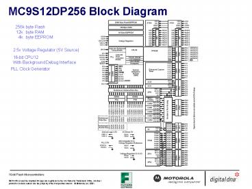
MC9S12DP256 Block Diagram
256k byte Flash 12k byte RAM 4k byte EEPROM
2.5v Voltage Regulator (5V Source)
16-bit CPU12 With Background Debug Interface
PLL Clock Generator
2
HCS12 Serial Interface Features
- 2 SCI Interfaces
- Up to 3 SPI interfaces
- SCI is Asynchronous Communication Port
- SPI is a Synchronous High Speed Communication
Port - Modular Architecture allows future expansion
- SCI SPI are similar to MC68HC11 with
enhancements - pins may be configured as general purpose I/O
- Loop mode operation for debugging
- SCI SPI have single-wire function
Enhancements 1- 1.56M baud _at_25MHZ clock (Max
Baud Rate (system/16) 2- Allows for single-wire
system 3- Receiver active flag allowing for
multi-transmitter synchronization. 4-
Additional break generation of 13 or 14 bit time
depending on 8 or 9-bit char length,
respectively. 5- Hardware parity generation and
checking.
3
Serial Communications Interface (SCI)
- 2 SCI interfaces
- Full-duplex operation
- Selectable Baud Rates derived from system clock
- Programmable 8-bit or 9-bit data format
- Separately enabled transmitter and receiver
- Idle line and address mark walk-up receiver
wake-up methods - Advanced data sampling technique
- Parity generation and checking
- Communication may be interrupt driven
4
SCI Features (Contd)
Receiver
Receiver DATA Register FULL FLAG
ERROR DETECT FLAGS
FRAMING
NOISE
OVERRUN PARITY
Receiver WAKE-UP FUNCTION (IDLE OR ADDRESS BIT)
Transmitter
- TRANSMIT DATA Register EMPTY FLAG
- TRANSMIT COMPLETE FLAG
- PARITY GENERATION
- BREAK SEND
5
SCI Block Diagram
Notice that SCI data rate limited to bus speed
divided by 16. 1.56 Mbit/sec maximum
6
Double Buffering
Transmitter
Receiver
DATA IN
P A R I T Y C H E C K
P A R I T Y G E N .
DATA
TDR BUFFER
T8
IN
DATA
RDR BUFFER
R8
SHIFT REGISTER
OUT
DATA OUT
- RDRF Flag sets each time
- new data is transferred from
- the serial shift register to the
- RDR Buffer.
- IDLE - Idle Interrupt Flag
- TDRE Flag sets each time new data is transferred
from the TDR Buffer to the transmit serial shift
register. - TC - Transmission Complete Flag
7
Serial Peripheral Interface (SPI)
8
Serial Peripheral Interface (SPI)
- Up to 3 High speed synchronous serial interface.
- Master mode and slave mode Master Bus/2 Slave
Bus/4 - Control of SPI operation during wait mode
- Primarily intended for on-board communication
- May be used for multi-processor communication
- Flexible clock format
- Full Duplexed operation
- Communication may be interrupt driven
Enhancements 1- Single wire communication (MIMO)
pin 2- Least or Most significant bit first 3-
Transmitter is double buffered. 4- Transmit
buffer empty IRQ flag 5- Baud rate of up to 12.5M
bit/sec _at_25MHZ
9
SPI Description
CPU Writes
MOSI
Transmit Buffer
MISO
SHIFT REG
SHIFT REG
SCK
RECEIVE REG
RECEIVE REG
SLAVE
MASTER
CPU Reads
Master initiates transfer
Master drives serial data clock to synchronize
transfer
SPI receiver is double buffered
10
SPI, System
MASTER
SLAVE
SLAVE
MISO
MISO
MISO
MOSI
MOSI
MOSI
SCK
SCK
SCK
SS
SS
SS
ENABLE
ENABLE
ENABLE
SIGNALS
MISO
MOSI
SCK
SS
DEVICE MODE
MASTER
INPUT
OUTPUT
OUTPUT
INPUT
SLAVE
OUTPUT
INPUT
INPUT
INPUT
MISO output is tri-stated until enabled by SS
11
Serial Peripheral Interface
Useful for
Communicating with simple peripherals such as LCD
Drivers, A/D Converters, etc.
1.
2.
Communicating with other MCU's (e.g. HC08, HC11,
HC12, HCS12, HC16, 6833x, etc (One master and
multiple slaves).
Description
A master and a slave device communicate by
shifting bits to each other's registers. Upon
completion of 8 bit shifts, the following occurs
1. A Status flag, SPIF, is set
2. An interrupt is asserted, if enabled
12
SPI Application Examples
HCS12 SPI
5V
0.1uF
SS0
MC14489
7-segment
7-seg. driver
display x 5
11 ANALOG INPUTS
AN10 AN9 AN8 AN7 AN6 AN5 AN4 AN3 AN2 AN1 AN0
M C 1 4 5 0 5 0
H C S 1 2
SS1
CS SCLK MOSI MISO
MC14489
7-segment
VOLTAGE PRESSURE TEMPRATURE
SS SCLK MOSI MISO
7-seg. driver
display x 5
5V
SS2
Photocell
0.2 uF
MC145050
MISO
ATD CLK
11 chan. A/D
MOSI
Gas Pedal
SCK
2MHZ OSC
Switches
Thermistors
13
Timer Module (ECT)
Enhancements 1- All 8-channels can be programmed
either as IC or OC. 2- Allow dual action
functionality on channel 0-3 when used as
input capture. 3- 4 8-bit or 2-16 bit pulse
accumulators 4- Delay counter to filter out
noise pulses on channel 0-3 when used as
input capture. 5- Delay counter to filter out
noise pulses on PA 0-3. 6- IC0-IC3 and PA0-3
have holding registers allowing for snap-shot
of all input channels when using latch mode
capabilities. 7- 16-bit modulus down counter that
can be used to transfer IC register and PA
registers to their holding registers when the
count reaches 0000. 8- Modulus counter in the
queue mode of the timer may be used as
periodic interrupt timer. 9- Main timer TCNT is
turned off out of reset. 10- Flexible Time Base
clock generation. 11- Toggle OC channel upon TCNT
overflow capability. 12- Fast flag clear
mechanism.
14
Timer Structure
PRE-SCALER PR20
M Clock
1 2 4 8 16 32 64 128
15...........................................0
TCNT CLK
Address Offset 0004, 05
.
TCNT
B0..........B7 B8..........B15
TEN
PIN
DATA BUS
PA PULSE Accumulator
TSCR1 - TIMER SYSTEM CONTROL REGISTER
R
R
R
R
TEN TSWAI TSFRZ TFFCA
0006
RST 0 0 0 0 0
0 0 0
R Reserved
1 - CLOCKS COUNTER ENABLE 0 - CLOCKS COUNTER
DISABLE
15
Timer, Prescaler, and Counter
REGISTERS
16 BIT FREE RUNNING /MODULO COUNTER
B15...............................................
..................................................
...........................B0
Address Offset 0004, 0005
1. TCNT
RST 0.......................................
..................................................
...............................0
B7................................................
......................B0
000F
TOF 0 0 0 0 0
0 0
2. TFLG2
RST 0 0 0 0 0
0 0 0
Timer Overflow Flag Write a 1 to clear
B7................................................
....................................B0
PRESCALER SELECTION
TOI 0 0 0 TCRE PR2 PR1
PR0
000D
3. TSCR2
DIVIDE BY
PR2 PR1 PR0
RST 0 0 0 0
0 0 0 0
1 2 4 8 16 32 64 128
0 0 0 0 1 1 1 1
0 1 0 1 0 1 0 1
0 0 1 1 0 0 1 1
1 - TIMER RESET BY OC7 MATCH 0 - COUNTER IS FREE
RUNING
1 - TIMER OVERFLOW INTERRUPT ENABLE 0 - TIMER
OVERFLOW INTERRUPT DISABLE
TCRE - ALLOWS FOR PULSE WIDTH MODULATION
FUNCTION.
RESERVED
16
Timer Operation
USEFUL FOR
- BASIS FOR ALL THE TIMING FUNCTIONS
- PROVIDING TIME INFORMATION TO PROGRAMS
DESCRIPTION
- THE E-CLOCK DRIVES A PRESCALER, DIVISIBLE BY 1
AND UP T0 128, WHICH IN TURN DRIVES A 16-BIT
COUNTER. - WHEN THE TIMER GOES FROM FFFF TO 0000
- THE TIMER OVERFLOW FLAG BIT IS SET
- AN OVERFLOW INTERRUPT MAY OCCUR
17
Timer Overflow Interrupt
FOR TIMER OVERFLOW
- TO CLEAR INTERRUPT WRITE 1 TO TOF BIT TFLG2. DO
NOT USE BIT MANIPULATION INSTRUCTIONS (SINCE RM/W
OPERATION). - TIMER OVERFLOW VECTOR USED.
RESET CONDITIONS
- TCNT IS INITIALIZED TO ALL ZEROES AND Disabled
- TIMER OVERFLOW INTERRUPTS ARE Disabled
- TC7 - TC0 REGISTERS ARE CLEARED
- TIMER OVERFLOW FLAG IS CLEARED
- PRESCALER IS 1
18
Output Compare Function
Provides a mechanism to output a signal at a
specific time
TCNT
- Set Pin
- Clear Pin
- Toggle Pin
- Inhibit Pin
Compare/Capture Unit 16-Bit Free-Running Counter
Action taken upon match of compare register with
counter
Pin OCx
Pin Control Logic
16-Bit Compare
TOCx
16-Bit Output Compare Register (programmed by
software)
Status Flag is set upon compare match
OCxF
Optional Local Interrupt Mask (Enabled through
software)
Interrupt Request to CPU
OCxI
UP TO 8 separate Output Compare Functions
Each Output Compare Function has its own Vector
and Controls
19
Output compare, OC7-OC0
- Output waveform control (software controlled)
- Elapsed time indicator (to external circuitry)
Useful for
Description
During each e-clock cycle, the output compare
registers are compared to the free-running
counter. If there is a compare then
The interrupt flag bit is set. In addition,
either or both of the following may occur
- The state of the associated output pin may be
changed - An interrupt is generated to CPU, if enabled
20
Output Compare, OC7
CONTROL OF MULTIPLE OUTPUT COMPARE PINS
USEFUL FOR
1.
CONTROL OF A SINGLE PIN BY TWO OUTPUT COMPARES
2.
(THUS, SHORT PULSES ARE POSSIBLE).
DURING EACH E-CLOCK CYCLE, THE OUTPUT COMPARE
DESCRIPTION
REGISTER 1 IS COMPARED TO THE FREE-RUNNING
COUNTER.
IF THERE IS A COMPARE THEN
1. THE INTERRUPT FLAG BIT IS SET
IN ADDITION, EITHER OR BOTH OF THE FOLLOWING MAY
OCCUR
1. THE STATE OF OUTPUT PINS OC7OC0
MAY BE CHANGED
2. AN INTERRUPT MAY OCCUR
OC7 CAN AFFECT MULTIPLE PINS (OC7OC0)
OC7 ACTION OVERRIDES ANY CONFLICTING OC7OC0
ACTION
FOR A GIVEN PIN.
21
Timer Toggle on Overflow
TTOV -Timer Toggle On Overflow Register
Address Offset 0007
TOV7 TOV6 TOV5 TOV4 TOV3 TOV2
TOV1 TOV0
RST 0...0
TOVx - TOGGLE ON TIMER OVERFLOW TOVx Toggles
output compare pin on overflow. This feature is
applicable only when channel is configured for
Output Compare Function.
22
Input Capture Function
Provides a mechanism to capture the time at
which an external event occurs
TCNT
Compare/Capture Unit 16-bit Free Running Counter
Rising Edges Falling Edges Any Edge Inhibit
TICx
Pin ICx
Edge
Delay Counter
16-bit Input Capture Latch
Edge Select Detect
16-bit Holding Register
ICxF
Status Flag is set upon capture
Interrupt Request to CPU
Optional Local Interrupt Mask (Enabled through
software)
ICxI
DLYCT - Delay Counter Control Register
Up to 8 separate Input Capture function, IC7 -
IC0 Each Input Capture Function has its own
Vector and Controls
Bit 7 6 5 4 3 2
1 0
Address Offset 0029
0 0 0 0 0 0
DLY1 DLY0
DLY10 - Delay Counter Values 00
Disabled 01 256 M Clocks 10 512 M
Clocks 11 1024 M Clocks
Note Delay Counter produces a Pulse at preset
clock count if the level of the input
signal is the opposite of the level
before the transition.
23
Input Capture, IC7-IC0
USEFUL FOR
1. MEASURING TIME BETWEEN EVENTS (OCCURING IN
HARDWARE)
2. REACTING TO REALTIME EVENTS
DESCRIPTION
INPUT CAPTURE EDGE DETECTORS SENSE WHEN AN EDGE
OCCURS ON THE PIN. IF AN EDGE OCCURS, THE
FOLLOWING MAY HAPPEN
- THE COUNTER VALUE GOES INTO THE INPUT
- CAPTURE REGISTER A STATUS FLAG IS SET.
- 2. AN INTERRUPT IS GENERATED TO CPU, IF Enabled.
24
IC/OC Select
TIOS - TIMER INPUT CAPTURE/OUTPUT COMPARE SELECT
REGISTER
0000
IOS7 IOS6 IOS5 IOS4 IOS3
IOS2 IOS1 IOS0
RST 0 0 0
0 0 0 0
0
IOSx 1 SELECT OC FUNCTION 0
SELECT IC FUNCTION
TSCR - TIMER SYSTEM CONTROL REGISTER
TEN TSWAI TSFRZ TFFCA
Reserved
0006
RST 00
TFFCA - TIMER FAST FLAG CLEAR ENABLE 0 TIMER
FLAG CLEARING NORMALLY 1 A READ FOR IC, A
WRITE OF OC REGISTER CAUSES
CORRESPONDING CHANNEL FLAG TO CLEAR
TSBCK - TIMER STOP IN DEBUG MODE 0 DO NOT
STOP 1 DISABLE TIMER IN DEBUG MODE
TSWAI - TIMER STOP IN WAIT 0 NORMAL
OPERATION 1 DISABLE TIMER IN WAIT MODE
TIMER ENABLE 1 - CLOCKS COUNTER ENABLE 0 - CLOCKS
COUNTER DISABLE
25
Pulse Accumulator
USEFUL FOR
1. EVENT COUNTING
2. GATED TIME ACCUMULATION
DESCRIPTION
IF PULSE ACCUMULATION IS Enabled, THEN HCS12
RESPONDS TO EDGES ON PAI BY INCREMENTING THE
8 OR 16-BIT PULSE Accumulator COUNTER.
EVENT COUNTING MODE
INPUT EDGES ON PAI INCREMENT THE 8/16-BIT COUNTER
GATED TIME ACCUMULATION MODE
THE 8/16-BIT COUNTER IS INCREMENTED BY AN E/64
CLOCK IF Enabled BY THE LAST EDGE ON PAI
IF THE SPECIFIED EDGE OCCURS, THEN
1. THE PULSE Accumulator FLAG BIT IS SET
IN ADDITION, THE FOLLOWING MAY OCCUR
1. THE COUNTER MAY BE INCREMENTED
2. THE PULSE Accumulator OVERFLOW BIT MAY SET
3. AN INTERRUPT IS GENERATED TO CPU, IF Enabled.
26
Pulse Accumulator Block Diagram
TCx PIN Logic
Delay Counter
PTx
D A T A B U S
POLARITY CONTROL
PIN
Edge Detector
8/16 BIT CNTR
SELECTED CLOCK
IRQ
DIV by 64
LATCH
Control Reg.
DLYCT - Delay Counter Control Register
Note 1 PTx may be used as Pulse Accumulator,
Input Capture or Output Compare pin. Where PTx
PT0 - PT3
Address Offset 0029
Bit 7 6 5 4 3 2
1 0
0 0 0 0 0 0
DLY1 DLY0
DLY10 - Delay Counter Values 00
Disabled 01 256 M Clocks 10 512 M
Clocks 11 1024 M Clocks
Note 2 Delay Counter produces a Pulse at preset
clock count if the level of the input
signal is the opposite of the level
before the transition.
27
Pulse Accumulator
Interrupts For Pulse Accumulator Input and
Pulse Accumulator Overflow.
To clear Interrupt write a 1 to PAIF or
PAOVF bits in TFLG2.
Do not use bit manipulation instructions
(since RM/W operation).
Pulse Accumulator or Pulse Accumulator
Overflow vector used
Reset conditions
- Pulse accumulator is disabled
- Event counter mode
- Falling edges(event counter mode) or PAI high
enables
(gated time accumulation mode)
- Interrupts are disabled
- Flag bits are cleared
28
Pulse Accumulator Modes
29
ECT Latch Mode
Latch Mode LATQ 1 Modulus Down-Counter
causes IC x PA x registers to transfer to
their corresponding holding registers when
Counter reaches 0000, or when Down-Counter is
written with 0000.. In this mode, IC
registers are transferred to their
holding register when ICLAT bit is written in the
MCCTL register
30
ECT Queue Mode
Queue Mode LATQ 0 An Input Capture x Event
causes the IC register to transfer
to corresponding Holding register x, and new
captured value is written to corresponding IC
register. This mode also causes the PA x to
transfer to its corresponding holding register
when IC holding register x is read. Modulus
Down-Counter in this mode may only be used to
generate periodic Interrupts.
31
Modulus Counter Registers
MCCNT - Modulus Down-Counter Count Register
Address Offset 0036, 37
Modulus Down-Counter may be used to generate
periodic Interrupts. It can also be used to latch
IC and PA registers to their holding registers.
MCCTL - Modulus Down-Counter Control Register
Address Offset 0026
MCZI - Modulus Counter Interrupt Enable MODMC -
Modulus Mode Enable 1 Counter is loaded with
last value written to Modulus Count Register. 0
Counter counts once from value written to it and
will stop at 0000. RDMCL - Read Modulus Down
Counter Load 1 Reads of Counter returns the
contents of the Load Register. 0 Read of
Counter returns current value of the present
count. ICLAT - Input Capture Force Latch
Action When Latch Mode is enabled, write 1 to
this bit causes IC3-IC0 and their corresponding
Pulse Accumulators to be latched into their
associate holding registers.
FLMC - Force Load Register into Modulus Counter
by writing 1 to this bit MCEN - Modulus
Down-Counter Enable 1 Modulus Counter
Enabled. 0 Modulus Counter Disabled. MCPR10
- Modulus Counter Prescaler Select 00 Div/1 01
Div/4 10 Div/8 11 Div/16
MCFLG - Modulus Down-Counter Flag Register
Address Offset 0027
POLF30 - First Input Capture Polarity Status 1
Input Capture x was caused by rising edge. 0
Input Capture x was caused by falling edge.
MCZF - Modulus Counter Underflow Interrupt
Flag. This Flag is set when Modulus Counter
reaches 0000. Write 1 to clear.
32
ABS Application Example
PT0
LF WHEEL RF WHEEL LR WHEEL RR WHEEL
SENSOR 1
SIGNAL CONDITIONING LOGIC
IC/PA
H C S 1 2
SENSOR 2
PT1
SIGNAL CONDITIONING LOGIC
IC/PA
PT2
SENSOR 3
SIGNAL CONDITIONING LOGIC
IC/PA
SENSOR 4
PT3
Any port pins may be used to switch
brake fluid pumps on and off.
SIGNAL CONDITIONING LOGIC
IC/PA
TIMER
PB1
BRAKE
FLUID
PB2
PUMP
PB3
SYSTEM
PB4
Timer Input Captures measure wheel rotation.
Send commands to brake fluid pumps to adjust
pressure.
33
Angle Based Engine ControlApplication Example
SENSOR SENSOR
PIN
INPUT CAPTURE
SIGNAL CONDITIONING LOGIC
H C S 1 2 T I M E R
PIN
INPUT CAPTURE
SIGNAL CONDITIONING LOGIC
PIN
SPARK PLUG SPARK PLUG FUEL INJECTOR FUEL
INJECTOR
OUTPUT COMPARE
SIGNAL CONDITIONING LOGIC
PIN
OUTPUT COMPARE
SIGNAL CONDITIONING LOGIC
PIN
OUTPUT COMPARE
SIGNAL CONDITIONING LOGIC
PIN
OUTPUT COMPARE
SIGNAL CONDITIONING LOGIC
34
PWM
Enhancements 1- 8 independent PWM channels 2-
Flexible clock generation 3- Left or center
aligned capability 4- Emergency shut down 5- Can
concatenate 2 PWM channels to provide a 16-bit
PWM function.
35
PWM Features
- 8 independent PWM channels with programmable
period and duty cycle. - 8-bit 8-channels or 16-bit 4-channels.
- Dedicated counter for each channel.
- Flexible clock generation ( A, B, SA and SB )
that covers wide range of frequencies. - Period and duty cycle are double buffered.
- Allows for immediate PWM update.
- Polarity is software selectable.
- Programmable center or left-aligned PWM output.
- Emergency shut down
36
PWM Clock Selection
- Independent PWM clocks A and B allow for two
different PWM frequencies
37
PWM Clock Generation
PWMPRCLK - PRESCALER CLOCK SELECT REGISTER
B 7 B6 B5 B4
B3 B2 B1 B0
00A3
0 PCKB2 PCKB1 PCKB0
0 PCKA2 PCKA1 PCKA0
RST 0 0 0
0 0 0 0
0
PCKA2
PCKB2
PCKB1 PCKB0 CLOCK B OUT
PCKA1 PCKA0 CLOCK A OUT
0 0 0
E
0 0 1
E/2 0 1
0 E4 0 1
1 E/8 1
0 0
E/16 1 0 1
E/32 1 1
0 E/64 1
1 1
E/128
PRESCALER SELECT FOR CLOCK A
PRESCALER SELECT FOR CLOCK B
38
PWM Clock Selection
PWMCLK - PWM Clock Select Register
B 7 B6 B5 B4
B3 B2 B1 B0
00A2
PCLK7 PCLK6 PCLK5 PCLK4 PCLK3 PCLK2
PCLK1 PCLK0
RST 0 0 0
0 0 0 0
0
PCLK7 - Pulse Width Channel Select
0 Clock B is the clock source for PWM channel
7 1 Clock SB is the clock source
for PWM channel 7
PCLK5 - Pulse Width Channel Select 0
Clock A is the clock source for PWM channel 5
1 Clock SA is the clock source for
PWM channel 5
PCLK6 - Pulse Width Channel Select
0 Clock B is the clock source for PWM channel
6 1 Clock SB is the clock source
for PWM channel 6
PCLK4 - Pulse Width Channel Select 0
Clock A is the clock source for PWM channel 4
1 Clock SA is the clock source for
PWM channel 4
PCLK3 - Pulse Width Channel Select
0 Clock B is the clock source for PWM channel
3 1 Clock SB is the clock source
for PWM channel 3
PCLK1 - Pulse Width Channel Select 0
Clock A is the clock source for PWM channel 1
1 Clock SA is the clock source for
PWM channel 1
PCLK2 - Pulse Width Channel Select
0 Clock B is the clock source for PWM channel
2 1 Clock SB is the clock source
for PWM channel 2
PCLK4 - Pulse Width Channel Select 0
Clock A is the clock source for PWM channel 0
1 Clock SA is the clock source for
PWM channel 0
39
PWM Scale and Alignment Control
PWSCALA PWM SCALE REGISTER A
B 7 B6 B5 B4
B3 B2 B1 B0
00A8
0 0 0 0
0 0 0 0
RST 0 0 0
0 0 0 0
0
Clock SA Clock A/ (2 PWMSCLA)
PWSCALB PWM SCALE REGISTER B
B 7 B6 B5 B4
B3 B2 B1 B0
00A9
0 0 0 0
0 0 0 0
RST 0 0 0
0 0 0 0
0
Clock SB Clock B/ (2 PWMSCLB)
PWMCAE - PWM ALIGN ENABLE REGISTER
B 7 B6 B5 B4
B3 B2 B1 B0
00A4
CAE7 CAE6 CAE5 CAE4 CAE3 CAE2
CAE1 CAE0
RST 0 0 0
0 0 0 0
0
CAEx 0 PWMx LEFT ALIGNED CAEx 1 PWMx CENTER
ALIGNED
40
PWM LEFT ALIGNED-OUTPUT
CLK SRC E or S
CENTR 0
PWMCNTx
GATE
UP/DOWN
R E S E T
FROM PORT P DATA REGISTER
DUTY CYCLE
8-BIT COMPARE PWDTYx
TO PIN DRIVER
M U X
S R
M U X
Q Q
PERIOD
8-BIT COMPARE PWPERx
PPOLx
PWENx
41
PWM CENTER ALIGNED-OUTPUT
CLK SRC E or S
CENTR 1
PWMCNTx
GATE
RESET
U P / D O W N
FROM PORT P DATA REGISTER
DUTY CYCLE
8-BIT COMPARE PWDTYx
TO PIN DRIVER
M U X
T
M U X
Q Q
PERIOD
8-BIT COMPARE PWPERx
PPOLx
PWENx
PPOL 0 PPOL 1
PWDTY
PWDTY
PWPER2
42
16-BIT PWM Concatenation
CLOCK SOURCE 7
PWCNT 6 PWCNT 7
PERIOD/DUTY COMPARE
PWM7
CLOCK SOURCE 5
PWCNT 4 PWCNT 5
PERIOD/DUTY COMPARE
PWM5
CLOCK SOURCE 3
PWCNT 2 PWCNT 3
- Channel concatenation is software selectable.
- Left aligned-output or center-aligned output
allowed in this mode. - Increase resolution and longer periods
PERIOD/DUTY COMPARE
PWM3
CLOCK SOURCE 1
PWCNT 0 PWCNT 1
PERIOD/DUTY COMPARE
PWM1
Note that on HC12, clock originates from sources
0, 2, 4, and 6.
43
PWM Channel Concatenation Control
PWMCTL - PWM Control Register
00A5
CON67 CON54 CON32 CON10
PSWAI PFRZ 0 0
CON67 - Concatenate Channel 6 and 7 PSWAI - PWM
Stops in Wait Mode 0 Normal
Operation CON45 - Concatenate Channel 4 and 5
1 Stop clock when MCU enter wait mode.
CON23 - Concatenate Channel 2 and 3 PFRZ -
PWM Counters stop in Freeze mode
0 PWM Counters continue to run in Freeze
mode CON10 - Concatenate Channel 1 and 0
1 Stop counters input clocks in Freeze mode
44
PWM Registers
PWMPOL - PWM POLARIY REGISTER
B 7 B6 B5 B4
B3 B2 B1 B0
00A1
PPOL7 PPOL6 PPOL5 PPOL4 PPOL3
PPOL2 PPOL1 PPOL0
RST 0 0 0
0 0 0 0
0
PULSE WIDTH POLARITY PPOLx 1 PWMx BEGINS
HI PPOLx 0 PWMx BEGINS LO
PWMEN - PWM ENABLE REGISTER
B 7 B6 B5 B4
B3 B2 B1 B0
00A0
PWMEN7 PWME6 PWMEN5 PWMEN4 PWMEN3 PWMEN2
PWMEN1 PWMEN0
RST 0 0 0
0 0 0 0
0
PWMENx 1, PWMx ENABLED PWMENx 0, PWMx DISABLED
45
PWM Registers
PWMCNTx - PWM Channel Counter x
Read/Write
00AC - 00B3
0 0 0
0 0 0
0 0
RST 00
PWMPERx - PWM Channel Period Register x
Read/Write
00B4 - 00BB
0 0 0
0 0 0
0 0
RST 11
PWMDTYx - PWM Channel Duty Register x
00BC - 00C3
0 0 0
0 0 0
0 0
Read/Write
RST 11
Where X channel 0 -channel7
46
PWM Shut Down Control
PWMSDN - PWM Shut Down Register
00C4
Read/Write
PWMIF PWMIE PWMRSTRT PWMLVL
0 PWMIN PWM7INL PWM7EN
RST 0.
0
PWM7EN PWM emergency shutdown Enable If this
bit is 1 the pin associated with channel 7 is
forced to input and the emergency shutdown
feature is enabled. All the other bits in this
register are meaningful only if PWM7ENA 1. 1
PWM emergency feature is enabled. 0 PWM
emergency feature disabled. PWM7INL PWM
shutdown active input level for CH 7. If the
emergency shutdown feature is enabled (PWM7EN
1), this bit determines the active level of the
PWM7channel. 1 Active level is high 0 Active
level is low PWM7IN PWM channel 7 input
status. This reflects the current status of the
PWM7 pin. PWMLVL PWM shutdown output Level. If
active level as defined by the PWM7IN input, gets
asserted all enabled PWM channels are immediately
driven to the level defined by PWMLVL. 1 PWM
outputs are forced to 1. 0 PWM outputs are
forced to 0
PWMRSTRT PWM Restart. The PWM can only be
restarted if the PWM channel input
is de-asserted. After writing a 1 to the
PWMRSTRT bit (trigger event) the PWM channels
start running after the corresponding
counter passes next counter 0 phase. Also if
the PWM7EN bit is reset to 0, the PWM do not
start before the counter passes 00. PWMIE PWM
Interrupt Enable If interrupt is enabled an
interrupt to the CPU is asserted. 1 PWM
interrupt is enabled. 0 PWM interrupt is
disabled. PWMIF PWM Interrupt Flag Any change
from passive to asserted (active) state or from
active to passive state will be flagged by
setting the PWMIF flag 1. The flag is cleared
by writing a 1 to it. 1 change on PWM7IN
input 0 No change on PWM7IN input.
47
A/D Converter
Enhancements 1- 8 or 10-bit resolution 2- A/D
results may be right justified, left justified
signed or unsigned. 3- External trigger pin maybe
used to initiate A/D conversion. 4- Digital
result may be mapped to conversion sequence in
FIFO mode. 5- Port AD pins can be used as analog
input or digital input. 6- Interrupt generation
with flag fast clear option.
48
Analog to Digital Converter
FEATURES
8/10 Bit Resolution. 7 usec, 10-Bit Single
Conversion Time. Sample Buffer Amplifier.
Programmable Sample Time. Left/Right Justified,
Signed/Unsigned Result Data. External Trigger
Control. Conversion Completion Interrupt
Generation. Analog Input Multiplexer for 8
Analog Input Channels. Analog/Digital Input Pin
Multiplexing. 1 to 8 Conversion Sequence
Lengths. Continuous Conversion Mode. Multiple
Channel Scans.
49
A/D Register Map
Note there are eight independent result registers.
50
A/D Clock Select/ Prescaler
Maximum A/D Clock 2.0 MHz (MININUM A/D
CLOCK .5 MHz)
PRS0-PRS4
Divide By 2
SYSTEM CLOCK
5-Bit Modulus Counter Prescaler
A/D Clock
ATDCTL4(HI) - A/D CONTROL REGISTER
Address offset 0004
SRES8 - A/D Resolution Select 1 Select 8-bit
Resolution 0 Select 10-bit Resolution
SAMPLE TIME SELECT
SMP 10
Sample Time
00
2 A/D Clock Periods
01
4 A/D Clock Periods
10
8 A/D Clock Periods
11
16 A/D Clock Periods
5-Bit Modulus Counter Prescaler - Controlled
by PR40 in A/D Control Register 0 - Divides
system clock by any integer from 2 to 64,
inclusive(PRS value 1) - If PRS40 0,
then prescaler is bypassed Note PRS40 must
not make A/D Clock gt 2 MHz.
51
Conversion Timing
A/D Clock
2, 4, 8, 16 Clocks
Always 2 Clocks
Conversion time calculation Examples (Assume
2MHZ A/D Clock) Example 1 Conversion Time
Initial Sample Time Programmed Sample Time
Resolution Period
2 2 10 14 A/D Clocks
7uSec Example 2 Conversion Time
Initial Sample Time Programmed Sample Time
Resolution Period
2 16 10 28 A/D Clocks
14uSec
52
A/D Control Registers
ATDCTRL2 - A/D CONTROL REGISTER 2
Address offset 0002
ASCIE - A/D Sequence Complete Interrupt Enable
1 Enable A/D Interrupts 0 Disable A/D
interrupts
ADPU - A/D Power-Up Enable/Disable 1 Apply
Power to A/D 0 Reduce power by disabling A/D
ASCIF - A/D Sequence Complete Interrupt Flag 1
Sequence complete interrupt 0 no interrupts
pending
AFFC - A/D Fast Conversion Complete Flag Clear
1 Fast Flag clear sequence 0 Normal Flag
clear sequence
AWAI - A/D Wait Mode 1 Enable Conversion in
CPU Wait 0 Disable Conversion in CPU Wait
ETRIGLE - External Trigger Level/Edge Control 1
Level Mode - Active Level Gate 0 Edge Mode
- Active Edge Mode ETRIGP - External Trigger
Polarity Control 1 Active High Level or
Rising Edge Active 0 Active Low Level or
Falling Edge Active ETRIGE - External Trigger
Mode Enable 1 External Trigger Enabled 0
External Trigger Disabled
53
A/D Control Registers (Contd)
ATDCTRL3 - A/D CONTROL REGISTER 3
Address offset 0003
FIFO - Result Register FIFO 1 Result
Registers do not Map to Conversion sequence 0
Result Registers Map to Conversion Sequence
Conversion Sequence Length Coding
54
A/D Control Registers (Contd)
ATDCTRL5 - A/D CONTROL REGISTER 5
Address offset 0005
CHANNEL SELECTION 0 0 0 Chan 0 -
- 1 1 1 Chan 7
DJM - Result Register Data Justification Mode 1
Right Justified Mode 0 Left Justified Mode
SCAN - Continuous Conversion Sequence Mode 1
Select Continuous Conversion Sequence ( 4 or 8 )
0 Select Single Conversion Sequence (
4 or 8 times stop )
DSGN - Signed/Unsigned Result Data Mode 1
Select Signed Result 0 Select Unsigned Result
MULT - Multiple Channel Sample Mode 1 Select
Multiple Channel Conversion Mode 0 Select
Single Channel Conversion Mode
Note A write to this register aborts current
conversion sequence and initiates a new
conversion sequence.
55
Result Registers
Left Justified Result Data
Address Offset 0010 - 0011 -
- - 001E - 001F
Right Justified Result Data
Address Offset 0010 - 0011 -
- - 001E - 001F
56
A/D Registers (Contd)
ATDSTAT - A/D STATUS REGISTER
Address Offset 0006
0007
- SCF - Sequence Complete Flag
- - Set at end of conversion sequence in single
conversion mode (SCAN 0) - and at the end of first conversion sequence in
continuous conversion mode (SCAN 1). - - A write to this register clears SCF flag when
(AFFC 0). - ETORF - External Trigger Overrun Flag
- -Sets if active edges occur while
conversion sequence in progress. - FIFOR - Sets when the Result Register has been
written before it was read by the CPU ( CCF was
not cleared). - CC20 - Conversion Counter
- 3-Bit counter that points to the next channel to
be converted in 4 or 8 count sequence. - CCF7 -CCF0 - Conversion Complete Flags for
individual A/D channels. - - Set upon end-of-conversion for each associated
A/D channel. - - Cleared when associated A/D result register is
read.
57
A/D Port Register
PORTAD1 - A/D PORT Data Register
Address Offset 000F
ADA7 ADA6 ADA5 ADA4 ADA3 ADA2 ADA1 ADA0
A T D P T
ATDDIEN - ATD Digital Input Enable
Note Any port pin may be used as A/D or as GP
Input.
58
BDLC CONTROLLER
- SAE J1850 Compatible
- 10.4Kbps VPW bit format
- Digital noise filter
- Collision detection
- Hardware CRC generation checking
- Receive and Transmit Block mode supported
- Supports 4X receive mode (41.6 Kbps)
- Digital loop-back mode
- In-frame Response (IFR) Types 0, 1, 2, and
- 3 supported
- Power-Saving Stop and Wait modes with Automatic
- Wakeup on Network Activity
- Interrupt Generation with Vector Lookup Table
59
BDLC Block Diagram
To J1850 Bus
Physical Interface performs wave shaping,
driving and digitizing of data
MUX Interface provides link between the BDLC
digital section and the analog Physical Interface
Protocol Handler responsible for encoding and
decoding of data bits and special message symbols
Rx/Tx Buffers provide storage for data received
and transmitted onto the J1850 bus
CPU Interface contains software addressable
registers and provides link between CPU and
Buffers
To CPU
60
J1850 References
1 SAE Vehicle Network for Multiplexing and Data
Communications Standards Committee, SAE J1850
Standard, Class B Data Communications Network
Interface Rev MAY94 2 SAE Vehicle Network for
Multiplexing and Data Communications Standards
Committee, SAE J2178/1, Class B Data
Communication Network Messages Detailed Header
Formats and Physical Address Assignments, Issued
1992-06-06 3 SAE Vehicle Network for
Multiplexing and Data Communications Standards
Committee, SAE J2178/2, Class B Data
Communication Network Messages Data Parameter
Definitions, Issued 1993-06-29 4 SAE Vehicle
Network for Multiplexing and Data Communications
Standards Committee, SAE J2178/3, Class B Data
Communication Network Messages Frame IDs for
Single Byte Forms of Headers, Issued
1993-09-07 5 SAE Vehicle Network for
Multiplexing and Data Communications Standards
Committee, SAE J2178/4, Class B Data
Communication Network Messages Message
Definitions for Three Byte Headers, Issued
1995-02 6 International Congress Exposition,
February 27-March 2, 1995, SAE SP-1070,
Automotive Multiplexing Technology, ISBN
1-56091-620-6 7 Delco Electronics, XDE-3160,
General Motors Class 2 Communications
Requirements, Original Release, Release May 1,
1993 8 Christopher A. Lupini, Introduction to
Vehicle Multiplexing, University Consortium for
Continuing Education (UCCE), November 1-3, 1995
Training Program
61
msCAN
Enhancements HCS12 FILTERING IS 2x THAT OF THE
HC08
62
msCAN Bus
- Features
- Up to 5 msCAN Modules (msCAN)
- 3 Tx message buffers each Automatically Mapped
- 5 Background Rx Buffers
- Programmable I/O modes
- Maskable interrupts
- Programmable loop-back for self test operation
- Independent of the transmission medium (external
transceiver is assumed) - Open network architecture
- Multimaster concept
Note msCAN 0 is multiplexed with BDLC
msCAN 4 is multiplexed with IIC.
63
CAN Specification
LATEST REVISION (version 2.0) DIVIDED INTO
PARTS A B - PART A CONSISTS OF THE PREVIOUS
SPECIFICATION REVISION (1.2) -
Standard 11-bit Identifier Field - No
specification for message filtering -
Layered architecture description based on Bosch's
internal model - PART B OUTLINES
ENHANCEMENTS TO THE CAN PROTOCOL, INCLUDING
- Extended 29-bit Identifier Field -
Some message filtering requirements -
Layer description based on ISO/OSI reference
model MINIMUM CAN REQUIREMENTS INCLUDE
COMPATIBILITY WITH SPECIFICATION VERSION 2.0,
PART A MOST CURRENT INDUSTRIAL APPLICATIONS
USE THE STANDARD (11-BIT) IDENTIFIER FORMAT
64
CAN Properties
- Serial communications protocol developed by
Bosch, initially for automotive multiplex wiring
systems - Message prioritization defined by the user
- Guaranteed minimum latency for highest priority
messages - Multi-master protocol utilizes non destructive
collision resolution to ensure the highest
priority message is transmitted onto bus - Flexible system configuration allows the user to
create the network which best fits the
application - Error detection and error signaling features are
built into the CAN protocol, along with automatic
re-transmission of corrupted messages - Distinction between temporary errors and
permanent node failures prevents faulty nodes
from causing long-term disruptions of network
traffic
65
msCAN - Layered Architecture
DATA LINK LAYER LOGICAL LINK CONTROL
(LLC) SUB-LAYER - Acceptance Filtering
- Overload Notification - Recovery
Management MEDIUM ACCESS CONTROL (MAC)
SUB-LAYER - Data Encapsulation/Decapsulati
on - Frame Coding (Bit Stuffing/Unstuffing)
- Medium Access Management - Error
Detection/Signaling - Acknowledgement
- Serialization/Deserialization PHYSICAL
LAYER - Bit Encoding/Decoding -
Bit Timing - Synchronization
66
msCAN12 Buffer Scheme
msCAN Receive / Transmit Engine
Internal Priority Scheduling
HCS12 FILTERING IS 2x THAT OF THE HC08
HCS12 Memory Mapped I/O
Rx Buffer
or 8 x 8 bits
Rx Buffer
5X FIFO
67
IIC
- Compatible with I2C Bus standard
- Multi-master operation
- Software programmable for one of 256 different
serial clock frequencies - Software selectable acknowledge bit
- Interrupt driven byte-by-byte data transfer
- Arbitration lost interrupt with automatic mode
switching from master to slave - Calling address identification interrupt
- Start and stop signal generation/detection
- Repeated start signal generation
- Acknowledge bit generation/detection
- Bus busy detection
- Low power modes support
- Shared with msCAN 4
68
IIC Functional Block Diagram
Address Module
IIC_Interrupt R_Data W_Data
SCL D_IN IN/OUT D_OUT
69
IIC Communication Protocol
Slave Address An address byte followed by 1-bit
R/W command to tell the Slave the desired
direction of data transfer. ACK Bit - Slave
Transfer Acknowledge. Stop Master generates a
Stop signal to free the bus. Repeat
Start Repeat Start is a Start signal without
generating a Stop signal to terminate
communication.
START signal is defined as a high-to-low
transition of SDA while SCL is high. A master may
initiate communication by sending a START signal.
This signal denotes the beginning of a new data
transfer (each data transfer may contain several
bytes of data) and brings all slaves out of their
idle states.
70
FLASH EEPROM
71
FLASH EEPROM
- 256K bytes of Flash made of four 64K byte
blocks - Single supply program and erase.
- Automated program and erase algorithm.
- Interrupt on command completion.
- All four flash blocks can be programmed and
erased in parallel. - Read-While-Write into different block.
- Fast sector erase and word program operation.
- Flexible protection scheme against accidental
program or erase. - Security feature to prevent intrusive access.
72
Memory Map Flash Control
0100 010F
Flash Control Registers
0000 0400 1000 4000 8000 C0
00 FF00 FFFF
Registers
4K EEPROM
30 - 3F Denotes contents of PPAGE Register
Page 3F
12K RAM
Page 3E
Flash Protect Low Area .5K, 1K, 2K, 4K
16K Flash (Fixed)
Page 3E
Page 31
Page 30
16Kx16 Flash Pages (Windowed)
Flash 0 Protection/Security Fields
Address
Description FF00 -FFF7 Backdoor
comparison key FF08-FF09
Reserved FF0A Flash block 3
protection FF0B Flash block 2
protection FF0C Flash block 1
protection FF0D Flash block 0
protection FF0E Reserved FF0F
Security Byte
Page 3F
16K Flash (Fixed)
Flash Protect High Area 2K, 4K, 8K, 16K
Vectors
Flash Protect High Area
73
Flash Control Registers
- All four Flash Blocks Occupy 16 Bytes In The
I/O Register Area. - Registers Are Divided Into Banked and Unbanked
- Banked Registers Are Selected With BLKSEL1
BLKSEL0 In FCNFG - Unbanked Registers Control State Machine Clock,
Security, Interrupts - Banked Registers Control Erasure, Programming,
Protection - Banked Registers Allow Erasure and Programming
All Four Blocks in Parallel
74
FLASH Security
- Memory Security Mechanism Prevents Unauthorized
Access To Flash and EEPROM. - Prevents Access via BDM or Expanded Bus Unless
Flash and EEPROM Are Erased. - Security Is Controlled By The Two LSBs of The
FSEC Register. - These Bits Are Loaded From Flash Location FF0F.
- Two Bits of Opposite Polarity Are Used To Prevent
Security Mechanism From Being Tricked. - Security Mechanism Can Be Temporarily Disabled,
But It Requires Firmware Support In The Target
Application. - 64-bit Access Key Ensures That Security Mechanism
Can Not Be Easily Disabled By A Hacker.
75
Memory Protection
76
EEPROM Features
- 4K Non-Volatile Electrically Erasable
programmable memory located _at_0000 - 0FFF. - Relocateable to any 4K Boundary (this is
required to utilize entire 4K) - Organized as 2048 by 16-bit Words to allow for
word size Read/Write and Programming - Erase Sector 4 bytes (2 words)
- Three-step MCU instructions sequence to program
or erase the EEPROM. - Single supply program and erase.
- Automated program and erase algorithm.
- Interrupt on command completion.
- Fast sector erase and word program operation.
- Flexible protection scheme against accidental
program or erase. - Programming voltage derived from VDD with
internal charge pump - Hardware Interlocks
77
EEPROM Module Registers
ECLKDIV - EEPROM Clock Divider Register
Address Offset 0000
EDIVLD EEPROM Clock Divider Loaded This bit is
set when the ECLKDIV register is written to. If
this bit is 0 the register has not been written
since the last reset. Trying to program or erase
the EEPROM without having written to this
register previously will result in an access
error and the command will not be executed. 1
Register has been written to since the last
reset. 0 Register has not been written to since
the last reset. PRDIV8 Enable Prescaler by 8 1
Enables a prescaler by 8 before feeding into
the ECLKDIV divider. 0 OSCCLK is directly fed
into the ECLKDIV divider. EDIV50 EEPROM
Clock Divider The combination of FDIV8 and
EDIV50 is used to divide the oscillator clock
down to a frequency of 150KHz - 200KHz.
This resulting clock, ECLK, is used to drive the
program and erase state machine. ECLK - Should
be set to 200KHZ regardless of system frequency.
78
EEPROM Protection
EPROT - EEPROM Configuration Register
Address Offset 0004
EEPROM Protection address size
EPOPEN Opens the EEPROM block or a subsection
of it for program or erase. 1 The EEPROM block
or subsections are enabled to program or erase. 0
The whole EEPROM block is protected. In this
case the other bits within the protect register
are dont care. EPDIS EEPROM Protection
disable This bit determines whether there is a
protected area at the higher end of the EEPROM
block address map. 1 Protection disabled 0
Protection enabled
79
EEPROM Command
ECMD - EEPROM Command Buffer Register
Address Offset 0006
ERASE Erase EEPROM Erases a EEPROM sector (4
bytes) or the whole EEPROM depending on the MASS
bit. Trying to erase a sector located in a
protected area will result in a protection
violation indicated by the PVIOL bit in the FSTAT
register being set. 1 Perform a sector erase if
MASS0 or a mass erase if MASS1. PROG Word
programming Trying to program a word located in a
protected area will result in a protection error
indicated by PVIOL set. ERVER - Enable Erase
Verify Verifies the EEPROM block is fully erased.
A successful verification will set the BLANK bit
in the FSTAT register. 1 Perform an erase
verify after mass erase.
MASS - Enables Mass Erase Perform a mass erase of
the selected 64K byte block. This bit works in
conjunction with the ERASE bit. If any protection
is active on the selected block, mass erase has
no effect and the PVIOL bit in the FSTAT register
is set. Write at anytime. 1 Perform a mass
erase of the whole block. 0 Perform sector
erase.
80
EEPROM Status
ESTAT - EEPROM Status Register
Address Offset 0005
CBEIF Command Buffers Empty Interrupt
Flag Indicates that the address, data and command
buffers are empty so that a new command sequence
can be started. The flag is cleared by writing a
1. By clearing the flag the command sequence is
launched. Writing a 0 aborts a command sequence
that has not yet been launched and sets the
ACCERR flag. 1 Buffers are ready to accept a
new command. 0 Buffers are full. CCIF
Command Complete Interrupt Flag Indicates that
there are no more commands pending. 1 All
commands are completed 0 Command in
progress PVIOL Protection violation Indicates
an attempt was made to program or erase an
address in a protected memory area. A subsequent
program or erase command cannot be executed while
this flag is set. The flag is also cleared by
writing a new, valid command after CBEIF is
cleared or when CCIF is clear. 1 A protection
violation has occurred. 0 no failure
BLANK Blank Verify Flag Indicates that the
EEPROM block is fully erased in response to an
Erase-Verify command. 1 EEPROM block fully
erased. 0 EEPROM block not fully erased.
These flags are cleared by 1 to them.
81
Access Errors
1. Writing to the EEPROM address space before
initializing ECLKDIV. 2. Writing a misaligned
word or a byte to the EEPROM address space. 3.
Writing to the EEPROM address space while CBEIF
is not set. 4. Writing a second aligned word to
the EEPROM address space before executing a
program or erase command on the previously
written word. 5. Writing to any EEPROM register
other than ECMD after writing an aligned word to
the EEPROM address space. 6. Writing a second
command to the ECMD register before executing the
previously written command. 7. Writing a MASS
erase command to ECMD while any protection is
enabled. See EPROT register description. 8.
Writing a sector erase command to ECMD while
protection is enabled for that sector. See EPROT
register description. 9. Writing to any EEPROM
register other than ESTAT (to clear CBEIF) after
writing to the command register. BLANK Blank
Verify Flag Indicates that the EEPROM block is
fully erased in response to an Erase- Verify
command. The flag is cleared by writing a 1. 1
EEPROM block fully erased. 0 EEPROM block not
fully erased.
Recommended
CrystalGraphics Presentations


