
Joining Nonoxide ceramics for use at high temperatures - PowerPoint PPT Presentation
1 / 22
Title: Joining Nonoxide ceramics for use at high temperatures
1
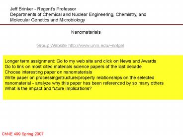
Jeff Brinker - Regents Professor Departments of
Chemical and Nuclear Engineering, Chemistry,
and Molecular Genetics and Microbiology
Nanomaterials
Group Website http//www.unm.edu/solgel
Longer term assignment Go to my web site and
click on News and Awards Go to link on most cited
materials science papers of the last
decade Choose interesting paper on
nanomaterials Write paper on processing/structure/
property relationships on the selected nanomateria
l - analyze why this paper has been referenced by
so many others What is the impact and future
implications?
2
The Scale of Things Nanometers and More
Things Natural
Things Manmade
1 cm 10 mm
10-2 m
Head of a pin 1-2 mm
The Challenge
1,000,000 nanometers
10-3 m
1 millimeter (mm)
MicroElectroMechanical (MEMS) devices 10 -100 mm
wide
Microwave
0.1 mm 100 mm
10-4 m
Human hair 60-120 mm wide
Microworld
0.01 mm 10 mm
10-5 m
Pollen grain
Red blood cells
Infrared
Red blood cells with white cell 2-5 mm
1,000 nanometers
Zone plate x-ray lensOuter ring spacing 35 nm
10-6 m
1 micrometer (mm)
Visible
Fabricate and combine nanoscale building blocks
to make useful devices, e.g., a photosynthetic
reaction center with integral semiconductor
storage.
0.1 mm 100 nm
10-7 m
Ultraviolet
Self-assembled, Nature-inspired structureMany
10s of nm
Nanoworld
0.01 mm 10 nm
10-8 m
10 nm diameter
Nanotube electrode
ATP synthase
10-9 m
1 nanometer (nm)
Carbon buckyball 1 nm diameter
Soft x-ray
Carbon nanotube 1.3 nm diameter
DNA 2-1/2 nm diameter
0.1 nm
10-10 m
Quantum corral of 48 iron atoms on copper
surface positioned one at a time with an STM
tip Corral diameter 14 nm
Atoms of silicon spacing tenths of nm
Office of Basic Energy Sciences Office of
Science, U.S. DOE Version 10-07-03, pmd
3
(No Transcript)
4
(No Transcript)
5
Doubling the density of transistors every 1 year
- (now 18 months) Today 106 transistors/mm2
6
(No Transcript)
7
(No Transcript)
8
(No Transcript)
9
Why are nanomaterials important ? PROPERTIES
SIZE MATTERS!!! -Smaller, faster, cheaper,
lighter weight, lower power -new size-dependent
functionality -band-gap engineering -magnetic
behavior -catalysis/molecular
recognition -adhesion. -Biological systems
are composed of nanoscale components and have
evolved to solve challenging engineering problems
(energy conversion, water purification,
self-repair.) as we learn from BIOLOGY
different operations work better at
different length scales?hierarchical structures
/materials - How do we make
Nano-materials??? TOP-DOWN or BOTTOM-UP??
FABRICATION PROCESSES are either additive
(bottom-up) or subtractive (top-down)
Can we achieve the functionality of a natural
biological system in a robust synthetic system???
10
sp3 hybridization tetrahedral
sp2 hybridization trigonal planar
graphite
11
(No Transcript)
12
Another Form of C60
13
(No Transcript)
14
Chiral (4,2)
15
Chiral (4,2)
16
(No Transcript)
17
(No Transcript)
18
Quantum Confinement
QD size becomes less than the nn Bohr radius
Energy levels discrete and size dependent-
addition or raction of one atom or electron
changes bandgap
19
Sol-gel chemistry provides a means to tune
fractal dimension (roughness Factor) and cluster
size (volume fraction porosity) enabling
systematic control of wetting
20
Aerogel-based SH film is optically transparent
with only nanoscale roughness yet contact angle
hystersis can be extremely low. Natural Systems
have dual-scale roughness.
Contact Angle Hysteresis
Growth ?? in each
frame is 0.2
B
A
Retraction
D
C
21
Combine sol-gel chemistry with molecular
self-assembly during evaporation ? EISA - Combine
EISA with top-down approaches and living cells to
develop greater levels of functionality
Low k dielectrics
Ultra low k - superhydrophobic
NC/silica arrays
EISA w CTAB
Understand collective electronic, photonic,
plasmonic, properties of metamaterials
Polymer/silica Sea shell mimetic nanocomposite
Aerogel w/o autoclaves
Sellinger et al., Nature 1998
Evaporation Inducedl self-assemby
Fan et al., Science 2004
Aerogels Vis Springback
Cavitation between SH surfaces
Understand long range hydrophobic forces
Sol-gel chemistry - with or w/o
structure-directing agents
Optical definition of nanoscale structure and
function
Singh et al. Nature, August 2006
EISA of photosensitive nanostructures
Doshi et al., Science 2000
Cell-directed Assembly (CDA)
J.AM Chem Soc 03
Understand EISA with added cells
Baca et al. Science July 2006
Evaporation driven processing provides a facile
route for nanostructure integration
22
EISA Background summary of several recent
advances/conclusions -in situ studies -Plasma-as
sisted atomic layer deposition EISA in presence
of living cells H2O/superhydrophobic interface
70 nm
Recommended
CrystalGraphics Presentations


