
3'2'4 Process Extensions - PowerPoint PPT Presentation
1 / 25
Title:
3'2'4 Process Extensions
Description:
(1)Double-level metal: Metal1 & Metal2. One layer for x-direction; ... Photoresist coating patterned using N-S/D Mask (Lightly-doped Drain) ... – PowerPoint PPT presentation
Number of Views:106
Avg rating:3.0/5.0
Title: 3'2'4 Process Extensions
1
3.2.4 Process Extensions
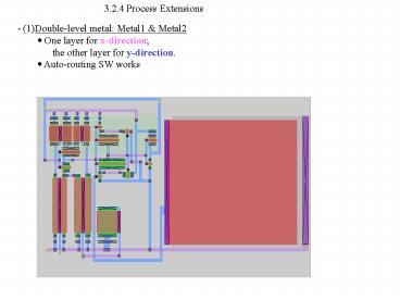
- (1)Double-level metal Metal1 Metal2
- One layer for x-direction the other
layer for y-direction. - Auto-routing SW works
2
3.2.4 Process Extensions
- (1)Double-level metal Metal1 Metal2
- One layer for x-direction the other
layer for y-direction. - Auto-routing SW works
- High power CMOS circuits (e.g., output driver)
can combine multiple metals for a thicker
conductor. - Two mask steps additional - Via hole M2
patterning
3
- (2) Silicidation
- Gate-poly reduced Rs by silicidation
- S,D diffusions reduced contact resistance
- Contact spiking prevented by silicidation
- Schottky diodes Pt, Pd silicide contacts
- Some silicides do not have Barrier Potential for
Schottky ex) TiSi - Gate poly after silicidation ? Rs 2 W/sq !
- Poly Resistor use Silicide block mask ! ?
complicates but
necessary for most Analog designs ! - If NSD diffusions are silicided, ? Rs 2 W/sq !
Not usable for Resistor.
Also needs Silicide Block Mask ! - If PNP has silicided Emitter region ? reduces b
! ? may need silicide block
mask.
4
- (3)Lightly Doped Drain (LDD) ? hot carrier
degradation - L 3mm NMOS ok for 5-10V PMOS ok for
15-20V - Increase depletion width to reduce E-field
- LDD to provide lighter-doped Drain near channel.
? Now, NMOS of for 10-20V
- No LDD for Short-channel FET as punch-through
occurs before hot
electron effect
5
- (4)Extended-Drain High-Voltage Transistors
- For High voltage devices with Vds gt 10-20V, Drain
region is
lightly doped NWELL ? asymmetric MOS. - Vbr gt 30V
- No Self-align process
- Thicker Gate oxide over High-field stress area
(thin oxides ruptures) - Thin, normal Gate oxide over other area for high
gm.
6
3.3 Analog BiCMOS
7
3.3 Analog BiCMOS
- Early 1980s ? Mixed-signal (both analog
digital) ICs. - 90-95 Digital, 5-10
Analog. - But, the small of devices consume the most
design time because of the
process inadequacies ! - ?
- Analog portion by tailor made components in late
1980s ! By mid 1990s, most analog by some kind
of BiCMOS process. - Analog BiCMOS ? mostly CMOS process, but
Bipolars, high-Rs Poly resistors, ?
Still an evolving process.
8
3.3 Analog BiCMOS
- Early 1980s ? Mixed-signal (both analog
digital) ICs. - 90-95 Digital, 5-10
Analog. - But, the small of devices consume the most
design time because of the
process inadequacies ! - ?
- Analog portion by tailor made components in late
1980s ! By mid 1990s, most analog by some kind
of BiCMOS process. - Analog BiCMOS ? mostly CMOS process, but
Bipolars, high-Rs Poly resistors, ?
Still an evolving process.
9
- 3.3.1 Essential Features
- High mask levels (expensive, time consuming, )
15 - 30 Masks ! - (1) NPN Bipolar Process Collector-diffused-isola
tion (CDI) - E B by successive counter-doping in NWELL.
- 3 Masks NBL, deep-N, and Base
10
(No Transcript)
11
3.3.1 Essential Features
- (2) Role of NBL
- reduces collector resistance
- blocks vertical punch-through in thin epi
process ? higher op. Voltage - suppresses parasitic substrate PNP action
- NBL is REQUIRED for lateral PNP
- So, BiCMOS will have NBL !
12
3.3.1 Essential Features
- (3) Deep-N
- Without this ? too high collector resistance ?
premature saturation for low-V op. ? - Most BiCMOS has it, maybe as process extension
13
3.3.1 Essential Features
- (5) Base diffusion of CDI NPN is a key step.
- Sets Gain, Vbr, VA,
- 1/ b DpNBW/DnNELp W2/2DntB
14
3.3.2 BiCMOS Fabrication Steps
- (1) Starting Silicon
- P (100)
- For NBL, need 20 mm-thick epitaxial Silicon
- Depletion width of resulting P/N must withstand
Vmax 30-50 V
15
3.3.2 BiCMOS Fabrication Steps
- (2) N-buried Layer
- Oxide growth ? NBL Mask ? Etch to open window
for NBL implant ? As or
Sb (n-type) implant ? Anneal - (3) Second P-Epilayer
- 10 mm-thick
- Epi grows at 45 deg. Angle wrt. 100
- Sb-dopants help reduce N-type auto-doping
(lateral)
16
3.3.2 BiCMOS Fabrication Steps
- (4) N-Well Diffusion and Deep-N
- oxide ? N-well Mask ? Phosphorus (n-type)
implants ? Driving diffusion, but ends
short of touching NBL ? oxide ? deep-N
Mask ? Heavy Phosphorus implant ? Driving
diffusion until 25 overlap between NBL and
deep-N, N-well. - Device parameters affected by N-well diffusion
- PMOS want Nwell moderately doped for
punch-through problem NPN wants Nwell
lightly doped for Collector drift region. - Compromised Minimum channel length L 2-3 mm.
17
3.3.2 BiCMOS Fabrication Steps
- (5) Base Implant (the third counter-doping)
- Oxide ? Base Mask ? Boron (p-type) Implant ?
Anneal (low high T) - b degrades due to triple counter-doping of Base
- Many Impurities in Base (p-epi N-well Boron
diffusion) ? Increases Recombination ?
Increases IB ? Reduces b.
18
3.3.2 BiCMOS Fabrication Steps
(6) Inverse Moat For Thick Field Oxide by LOCOS
same as in Poly-gate CMOS
19
3.3.2 BiCMOS Fabrication Steps
- (7) Channel Stop Implants
- Same as in Poly-gate CMOS
- Blanket Boron (p-type) implant ? followed
by patterned Phosphorus (n-type) implants.
20
3.3.2 BiCMOS Fabrication Steps
- (8) LOCOS Dummy Gate Oxide
- Dummy Gate Oxide to remove unwanted Nitride
residue
21
3.3.2 BiCMOS Fabrication Steps
- (9) Vt Adjust
- Single Boron Vt-adjust implant ?
- Raises Vtn
- Lowers Vtp
- Photoresist ? pattern with Vt mask (only MOS
regions) ? Remove Dummy Gate Oxide ?
300-A Gate Oxide.
22
3.3.2 BiCMOS Fabrication Steps
- (11) Polysilicon Gate
- Intrinsic Polysilicon ? heavy Phosphorus doping
(N-type) by
blanket implant ? Poly1 Mask
23
3.3.2 BiCMOS Fabrication Steps
- (12) S/D Implants
- BJTs with Vbr 10-20V
- NMOS
- Photoresist coating ? patterned using N-S/D Mask
(Lightly-doped Drain) ? lightly Phosphorus
(N-type) doping, self-align by Poly-Gate ?
coat second Photoresist ? pattern by N S/D Mask
? N Drain to the edge of Oxide Spacers - PMOS
- P S/D directly after the Sidewall Spacers.
- 10-20V
- Sidewall spacers increase L for PMOS ?
So, plan for smaller Ld, drawn length.
24
3.3.2 BiCMOS Fabrication Steps
(12) S/D Implants
25
3.3.2 BiCMOS Fabrication Steps
Recommended
CrystalGraphics Presentations


