
SAMPLE LAYOUT RULES Appendix C - PowerPoint PPT Presentation
1 / 10
Title:
SAMPLE LAYOUT RULES Appendix C
Description:
SAMPLE LAYOUT RULES (Appendix C) Simplified (not up to date) layout rules in ... makes vert. NPN, lat. PNP, and sub. PNP. 3. Layout Rule Syntax 'LAYER1 width N um' ... – PowerPoint PPT presentation
Number of Views:898
Avg rating:3.0/5.0
Title: SAMPLE LAYOUT RULES Appendix C
1
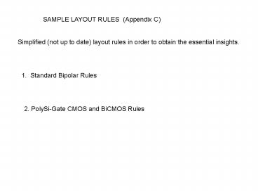
SAMPLE LAYOUT RULES (Appendix C)
Simplified (not up to date) layout rules in order
to obtain the essential insights.
1. Standard Bipolar Rules
2. PolySi-Gate CMOS and BiCMOS Rules
2
1. Standard Bipolar Rules
- 30-V process, single P iso,
- modern process uses Up/Down iso for smaller
isolation spacing - Key electrical parameters below
3
1. Standard Bipolar Rules, contd.
- baseline process 8 coding layers (in layout
editors) NBL, Tank, DeepN, Base, Emit, Cont,
Metal1, POR - POR Protective Overcoat Removal --- also
defines Protective Overcoat - TANK also codes openings in the Iso Diffusion
- BOI (Base Over Isolation) automatically
generated from TANK layer
Coding Grid 2 um assumed.
4
1. Standard Bipolar Rules, contd.
- HSR High Sheet Resistor
- Schottky Contact
5
2. PolySi-Gate CMOS and BiCMOS Rules
- 10 V, N-well, poly-gate CMOS as an example
- LDD NMOS, min. channel L 3 um
- SDD PMOS, min. channel L 4 um
- Both NMOS and PMOS have N-type gate Poly
- Single Boron Vt-adjust implant
- Thick-field threshold is safely above op. volt.
- CMOS latchup minimized by P sub and NBL
Typical parameter values
- cant fab Schottky DiodeTi-silicide is used for
all metalsto minimize contact R
6
2. PolySi-Gate CMOS and BiCMOS Rules, contd.
- baseline process 11 masksNWELL, MOAT, NSD,
PSD, CHST, POLY1, CONT, METAL1VIA, METAL2, POR - 9 Coding Layers for 11 masksNWELL, NMOAT,
PMOAT, POLY1, CONT, METAL1, VIA,METAL2, POR - NMOAT gt MOAT NSD
- PMOAT gt MOAT PSD
- NWELL MOAT gt CHST
- coding grid 0.5 um
7
2. PolySi-Gate CMOS and BiCMOS Rules, contd.
- POLY2 Extension 2nd Poly layer deposited as
near-intrinsic poly Si, - Poly R Poly2 doped with PSD
- Poly Cap POLY1 \ thin oxide-nitride-oxide \
POLY2
8
2. PolySi-Gate CMOS and BiCMOS Rules, contd.
- Analog BiCMOS Extension 3 more Masks NBL,
DEEPN, BASE - Coding layer BASE gt MOAT BASE masks
- NBL forces a 2nd epi
- makes vert. NPN, lat. PNP, and sub. PNP
9
3. Layout Rule Syntax
LAYER1 width N um
LAYER1 spacing to LAYER1 N um
LAYER1 overlap LAYER2 N um
10
3. Layout Rule Syntax, contd
LAYER1 overhang LAYER2 N um
LAYER1 extends into LAYER2 N um
Recommended
CrystalGraphics Presentations


