Pcb Design PowerPoint PPT Presentations
All Time
Recommended
Synergise PCB Inc, was found in 2002 at USA with a firm commitment to provide best quality PCBs. FPCs & PCBA to match the international standards (IPC Class-II & III) in the designing and manufacturing. Visit: http://synergisepcb.com/
| PowerPoint PPT presentation | free to download
A MUST READ: PCB MATERIAL GUIDE Before we talk about PCB material, let’s started with a PCB introduction.PCB is a self-contained component of interconnected units found in gadgets ranging from ordinary beepers or pagers to complex radar and computer programs. A thin layer conducting substance printed or deposited on the insulating board called the substrate is used to develop circuits. The specific electronic units are put on the substrate’s surface, which is then soldered to the interlocked circuits. It is common to have PCB performing one role, for instance, a signal amplifier or a number of functions. There are main types of PCB construction. These include: Single-sided PCB Double-Sided Multi-layered
| PowerPoint PPT presentation | free to download
The Global PCB Design Software market size is estimated to reach $5.8 billion by 2027, growing at a CAGR of 10.5% during the forecast period 2022-2027, owing to the increasing adoption of complex PCBs for a variety of applications like schematic capture, growing penetration of communication devices & availability of open source software and so on.
| PowerPoint PPT presentation | free to download
With the use of a rigid flex PCB(rigid FPC), flexible circuit substrates and rigid circuit substrates are covered together. Rigid-flex PCBs cross the limits of conventional rigid PCBs and the one of a kind properties of flex circuits that utilization high-flexibility electrodeposited or moved strengthened copper conductors photograph carved onto a flexible protecting film. Flex circuits incorporate stack-ups produced using a flexible polyimide, for example, Kapton or Norton and copper-covered together through warmth, acrylic cement, and weight.
| PowerPoint PPT presentation | free to download
The Department of Electronics & Communication Engineering (ECE) at K.Ramakrishnan College of Technology, Trichy, recently organized a highly beneficial Value Added Course on PCB Design. Kasthuri, an experienced professional, conducted this event. The primary aim of the course was to provide IInd ECE students with practical knowledge and hands-on experience in PCB (Printed Circuit Board) design. Further, it is an essential skill in the field of Electronics & Communication Engineering.
| PowerPoint PPT presentation | free to download
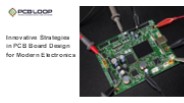
A successful electronic product relies heavily on a well-thought-out PCB board design. PCBLOOP is committed to providing cutting-edge design solutions that cater to the diverse needs of our clients. Our team is skilled in creating layouts that maximize space and improve signal integrity, ensuring that your circuits operate with optimal efficiency. We handle every aspect of the design process, from schematic capture to component placement, focusing on reducing noise and potential interference. With PCB board design playing a crucial role in the final product’s performance, partnering with experts like PCBLOOP ensures a smooth transition from design to manufacturing.
| PowerPoint PPT presentation | free to download
Pcbsky is located in Guangdong of China, the world's Printed Circuit Board manufacturing center. There are a large number of experienced pcb's technicians and perfect supply chain and so on, tends to perfect the outside environment, and therefore we have the rest of the world cannot compare with a congenital condition. More important than these, we can provide a better service and higher process capability.
| PowerPoint PPT presentation | free to download
PCBSky is a professional PCB & Flex PCB company in China, specializing in Quick Turn PCB & Prototypes. We are not just a PCB Maker, but rather a full-service PCB Supplier. We are not just a rigid PCB Factory, but also a Flexible Circuit(FPC) Manufacturer. Pcbsky is located in Guangdong of China, the world's Printed Circuit Board manufacturing center. There are a large number of experienced pcb's technicians and perfect supply chain and so on, tends to perfect the outside environment, and therefore we have the rest of the world cannot compare with a congenital condition. More important than these, we can provide a better service and higher process capability.
| PowerPoint PPT presentation | free to download
1. PCB Designer 2. Print PCB Mask ( ) 3. 4.
| PowerPoint PPT presentation | free to view
PCB is one of the leading PCB suppliers that have provided high quality electronic equipment's for growing industries. We have many years of experience in this field. If you want to take benefit from us then, visit our website.
| PowerPoint PPT presentation | free to download
Microprocessor PCB Design by: Tuan Hung Huynh April 3, 2006 Outline Background Design Process Application Results Purpose Designing computer circuits and software for ...
| PowerPoint PPT presentation | free to download
The designers at PNC have experience with both high power and high frequency RF and microwave PCB layout designs. Because they work closely with the manufacturing team, they know what is possible to achieve with the thick copper layers used in today’s compact LED and motor controllers, and they know what it takes to maintain consistent dielectric properties in the substrates, needed for predictable RF performance. Let them help you with your design.
| PowerPoint PPT presentation | free to download
Live project-based PCB & Circuit Design Training in Gurgaon at APTRON is an excellent choice for engineering students and professionals looking to enhance their skills in circuit design and PCB layout. The benefits of this course, such as industry-relevant curriculum, hands-on experience, expert trainers, state-of-the-art infrastructure, and placement assistance, make it a valuable investment in your career.
| PowerPoint PPT presentation | free to download
Altium Designer is considered the epitome of EDA tools for hardware design engineers when it comes to professional schematic and PCB design. It is inclusive and encompassing as far as all the steps in the design and management process are concerned.
| PowerPoint PPT presentation | free to download
Gold plating on PCBs enhances electrical conductivity, ensures corrosion resistance, and prolongs the lifespan of electronic components, ideal for achieving reliable performance and durability in advanced electronic applications.
| PowerPoint PPT presentation | free to download
PCB Design Services By TronicsZone In Low Cost
| PowerPoint PPT presentation | free to download
GREATPCB is a well-known turn-key PCB(1-30 layers) & PCB manufacturing service for low- to mid-volume electronic contract manufacturing, including PCB fabrication, sourcing of components, and complete electronic PCB assembly. With a state-of-the-art facility and modern technology.
| PowerPoint PPT presentation | free to download
Pcb assembly manufacturing: This article discusses about the benefits of employing contract PCB assembly manufacturing services. All electronic gadgets require printed circuit boards to get a compact size. The process of manufacturing printed circuit boards involves multiple stages. It begins with designing, setting up of the segments, connecting them together and testing using highly standardized development techniques. View more: https://www.greatpcb.com/pcb-assembly/
| PowerPoint PPT presentation | free to download
Are you someone who works in manufacturing or repairing electronic gadgets? Do you need the best quality PCB for your electronic instruments? If these questions have answers in the affirmative sense then you need to consider the best company providing the best circuit boards in the business. View More: http://www.greatpcb.com
| PowerPoint PPT presentation | free to download
Companies involved in PCB assembly manufacturing offer innovative solutions for various industries at cost-effective rates. Are you aware of the vital role played by PCBs? The full form of PCB is a printed circuit board. They are crucial components used by people worldwide. They are necessary for a broad array of applications in the industrial sector. PCBs are structures that link electronic components. The material used in nonconductive by nature. The etching of pads, lines and a host of features are done on copper sheets.
| PowerPoint PPT presentation | free to download
Pcb assembly china: Printed boards are an essential component of an electronic product. It is impossible to design any product without printed circuit boards. It is a non-conductive material connecting the electrical components to form a final product. Some of the components like resistors; capacitors are soldered onto the board to get the desired product. The application of single-sided, multilayer, or double-sided has gone a long way. Some of the applications of the boards are: View more: https://www.greatpcb.com/pcb-assembly/
| PowerPoint PPT presentation | free to download
PCB layout performs a primary role in the design for manufacturing of a printed circuit board. The layout procedure produces a visual reflection of the circuits that is essential to manufacture a PCB. Vayo offer design for manufacturing for PCB layout. Contact us today. Vayo Design For Manufacturing: - http://www.vayoinfo.com/
| PowerPoint PPT presentation | free to download
PCB Design for 1 Gbps. ECE 4006. Dr Brooke. Overview. What signals are being routed? ... Connect shields together. Balanced = equal and opposite. That is for ...
| PowerPoint PPT presentation | free to download
PCB Design for 1 Gbps ECE 4006 Dr Brooke Overview What signals are being routed? How can you route those signals? How to apply routing to PCB? PCB design techniques ...
| PowerPoint PPT presentation | free to download
PNC Inc. provides PCB design & layout services from schematics, a sample PC board or films.
| PowerPoint PPT presentation | free to download
The PCB Design Software Market size will be XX million (USD) in 2022 in China, from the XX million (USD) in 2016, with a CAGR (Compound Annual Growth Rate) XX% from 2016 to 2022.
| PowerPoint PPT presentation | free to download
VISIT HERE @ https://www.grandresearchstore.com/information-and-communication-technology-and-media/global-pcb-design-software-market-research-report-2017 This report provided by GrandResearchStore is about,PCB Design Software in Global market, especially in North America, Europe, China, Japan, Southeast Asia and India, focuses on top manufacturers in global market, with capacity, production, price, revenue and market share for each manufacturer, covering Mentor Graphics Candence Zuken Altium CadSoft Novarm Shanghai Tsingyue
| PowerPoint PPT presentation | free to download
You want to think about and ask which technology they are using when it comes to creating their devices like the 1-12 layer rigid-flexible PCB. Ensure that they are using the latest technology and not something that is outdated.
| PowerPoint PPT presentation | free to download
PCB design & PCB editor courses are conducted by CADD SCHOOL in Chennai. OrCAD software training is provided by CADD SCHOOL in Chennai. CADDSCHOOL is a capture/pspice training institute in Chennai. OrCAD software training is syllabus based and field wise contents are given by CADDSCHOOL in Chennai.
| PowerPoint PPT presentation | free to download
That is our designed purpose of DFT (design for testability). For end customer, the DFT (design for testability) logic present on the device is a repetitive further justify the need of DFT (design for testability) logic, think about an example where an organization needs to offer 1 Million chips to the client. For design for testability contact to vayoinfo @ http://www.vayoinfo.com/design-for-testability/
| PowerPoint PPT presentation | free to download
PCB design & PCB editor courses are conducted by CADD SCHOOL in Chennai. OrCAD software training is provided by CADD SCHOOL in Chennai. CADDSCHOOL is a capture/pspice training institute in Chennai. OrCAD software training is syllabus based and field wise contents are given by CADDSCHOOL in Chennai.
| PowerPoint PPT presentation | free to download
Complete report on PCB Design Software market spread across 68 pages providing 4 company profiles and 2 tables and 29 figures is now available at http://www.marketreportsonline.com/contacts/purchase.php?name=567047.
| PowerPoint PPT presentation | free to download
Design for manufacturing, making use of a knowledgeable design staff, improves return on general venture investment by developing efficient, repeatable, trusted items and preventing expensive item problems. Design for manufacturing will improve the high quality of an item from the starting of investment. Vayo provide the best DFM Software, check out design for manufacturing at http://www.vayoinfo.com/
| PowerPoint PPT presentation | free to download
Printed circuit boards with high-speed chips and microwave PCB structures have numerous parameters that differ significantly from those of conventional, rigid and flexible printed circuit boards. These differences are explained in IPC-6018B, Qualification and Performance Specifications for Radio Frequency (Microwave) Printed Circuit Boards. “High frequency” is one of the three primary classifications of circuit boards of the IPC (the other two classifications are “rigid” and “flexible” circuit boards).
| PowerPoint PPT presentation | free to download
In easiest form, Design for Testability is a process, which allows a design to turn into testable after production. “Extra” sense which we put combined with the design reasoning during setup process, which helps post-production screening. Post-production testing is required because, the method of developing is not 100% error free. Visit design for testability at http://www.vayoinfo.com/design-for-testability/
| PowerPoint PPT presentation | free to download
It is always important to hire only experienced and reliable PCB manufacturers from India to manufacture your PCBs, so that every design rule is thoroughly followed, thus ensuring safety and performance.
| PowerPoint PPT presentation | free to download
Pcb assembly manufacturing: In modern times the use of PCBs in the world of electronics has skyrocketed. Options exist in the form of single sided, double sided and multilayer settings. You can avail of rigid, flexible, or a combination of both rigid and flexible elements. View more: https://www.greatpcb.com/pcb-assembly/
| PowerPoint PPT presentation | free to download
Maintaining high speed PCB design quality from the driver to the collector on the PCB is not an easy task. One of the most testing issues is dealing with the engendering deferral and relative time postpones bungles. To deal with the time delays, we have to realize how to figure follow length from time postpone an incentive to execute the PCB support steering as needs are. Let me show you the procedure. The high-frequency PCB design also requires selective material for PCB.
| PowerPoint PPT presentation | free to download
Although PCBs are designed to be used in electronics that can heated up during operation, those PCBs that need to be used in extremely high environments need to be designed with special considerations.
| PowerPoint PPT presentation | free to download
The vision of Livewire is huge and will be better than any other IT/ITES training institute provider, encourage new minds willing to excel in MATLAB, Numerical Computation, Ic Design Analysis & PCB Editor.
| PowerPoint PPT presentation | free to download
The vision of Livewire is huge and will be better than any other IT/ITES training institute provider, encourage new minds willing to excel in MATLAB, Numerical Computation, Ic Design Analysis & PCB Editor.
| PowerPoint PPT presentation | free to download
Power integrity could be a significant issue in the case of power supplied. You can optimize the power integrity of your system by designing an appropriate PCB by using these four simple tips.
| PowerPoint PPT presentation | free to download
This course is an introductory course to designing Printed Circuit Boards and ... All values are in basic SI units [Ohm, Farad, Henry,Volt, Ampere] ...
| PowerPoint PPT presentation | free to view
A FEI/ADE Initiative, funded by the DTI. Welcome to Tweed Horizons 'Progress through Partnership' ... Initiative by design group within PCIF. Support by DTI for ...
| PowerPoint PPT presentation | free to view
PCB & Circuit Design Training in Delhi at APTRON Delhi is sure to be a game-changer in your journey towards success. So, enroll now and take the first step towards a brighter future in the world of electronics!
APTRON's PCB & Circuit Design Training in Noida provides placement assistance to the students. The training institute has tie-ups with various electronics companies in Noida and other cities, which helps the students to get placed in top-notch companies. The placement team also provides interview preparation and resume building sessions to the students.
Explore a wide range of PCB boards at SQPCB, designed for various electronic needs. Our high-quality, reliable boards ensure optimal performance for your projects. Visit sqpcb.com.
| PowerPoint PPT presentation | free to download
http://aptronnoida.in/summer/pcb-circuit-design-6-weeks-project-training-noida.html PCB Circuit Design Summer Training In Noida is coordinated by Aptron Noida. Aptron Noida is a main modern preparation establishment in Noida and Delhi and Gurgaon, gwalior, jaipur, lucknow. We give most learning conditions to significant innovation courses at reasonable costs. The best PCB Circuit Design 6 Weeks Summer Training In Noida gives the best specialized IT preparing for the applicable courses. We give fundamental and progressed PCB circuit configuration preparation in Noida with fitting functional information. At Aptron Noida, PCB circuit configuration preparation is given by industry specialists matured 8-10.
At Anzer, we provide top-notch PCB assembly services in the United States. Our state-of-the-art facilities and experienced team ensure the highest quality and reliability for your printed circuit board assembly needs
| PowerPoint PPT presentation | free to download
PCB adapter is a small electronic component that provides a connection between two different types of circuits. It is an important component in the electronics industry as it enables compatibility between different types of circuits and devices. PCB adapter comes in various types, and each type is designed to suit specific applications.
| PowerPoint PPT presentation | free to download
PCB microscopes come with features like digital imaging, camera attachments, and measurement capabilities, allowing users to capture images or videos of the PCB under examination and make precise measurements of components.
| PowerPoint PPT presentation | free to download
PCB microscope is a specialized tool that combines high magnification, clarity, and various adjustable features to facilitate the inspection, analysis, and troubleshooting of printed circuit boards. It is an essential instrument for professionals in the electronics industry who strive for precision and accuracy in their work.
| PowerPoint PPT presentation | free to download
PCB microscopes come with features like digital imaging, camera attachments, and measurement capabilities, allowing users to capture images or videos of the PCB under examination and make precise measurements of components.
| PowerPoint PPT presentation | free to download
PCB Design & Layout Tips Ref: Johnson, H., High-Speed Digital Design. Prentice Hall, 1993 PCB Checklist Do I have header pins for debugging? Do I have convenient VCC ...
| PowerPoint PPT presentation | free to download


