Superlattices PowerPoint PPT Presentations
All Time
Recommended
1st International Conference on Quantum Photonic Science Nonlinear Magneto-Optical Studies in Magnetic Superlattices and Magnetic Nano Structures
| PowerPoint PPT presentation | free to download
Dept de F sica/CCMM, Faculdade de Ci ncias Univ. Lisboa, Portugal ... Laboratoire des Mat riaux et du G nie Physique, ENSPG, France. M. Rosina and K. Frohlich ...
| PowerPoint PPT presentation | free to view
Observation of negative differential conductivity (NDC) due to 'Bloch ... vdr = D /(eFt) t -1 F-1, with L = D /(eFt), for wB 1/t; Hopping regime. vgrmax/2 ...
| PowerPoint PPT presentation | free to view
Optical properties of (SrMnO3)n/(LaMnO3)2n superlattices: an insulator-to-metal transition observed in the absence of disorder A. Perucchi SISSI, the IR beamline of ...
| PowerPoint PPT presentation | free to download
Large valence band splitting due to combination of deformation and quantum ... Eg=1.471eV, Valence band splitting Ehh1 - Elh1 = 60 meV, Maximal polarization ...
| PowerPoint PPT presentation | free to view
Neutron scattering studies of magnetic semiconductor thin films and ... Polarized neutrons and the in-plane magnetic anisotropy in EuS/PbS & EuS/YbSe. x=1 ...
| PowerPoint PPT presentation | free to view
University of Houston GaSb rich InAs rich The objective of this research is to understand the structural and optical properties of the nanowires formed by lateral ...
| PowerPoint PPT presentation | free to download
Lecture 3: optical phenomena in QWs and Superlattices. Recapitulation: optical transitions in semiconductors ... Probability for an optical transition between ...
| PowerPoint PPT presentation | free to view
Tunnelling Structures 4.3. Superlattices 4.1. Quantum Wells Nanophysics II Michael Hietschold Solid Surfaces Analysis Group & Electron Microscopy Laboratory ...
| PowerPoint PPT presentation | free to download
MURI - Integrated Nanosensors Ivan K. Schuller UCSD Characterization of InAs/GaSb Superlattices for IR Imaging Objective: Develop efficient InAs/GaSb IR detectors
| PowerPoint PPT presentation | free to download
The Key system has a stainless steel bell jar, a cryopump, gas supply system, ... Superlattices for x-ray reflectivity (High Z/Low Z)xn for high x ray contrast. ...
| PowerPoint PPT presentation | free to view
Electrical switching and memory phenomena in redox dendrimer multilayer ... Document presentation format: On-screen Show ... Hard Drives HDD technology HDD ...
| PowerPoint PPT presentation | free to view
of Thermal Conductivity of Si/SiGe Nanowire Superlattice ... Calculate k from q Repeat for different supercell sizes (for convergence) and different compositions, ...
| PowerPoint PPT presentation | free to download
Title: New Sample PL & PLE Author: toshi Last modified by: ihara Created Date: 7/5/2004 2:33:05 PM Document presentation format:
| PowerPoint PPT presentation | free to download
Version 3.0 X pert Epitaxy Functionality Graphics for single scans, area scans and wafer maps Peak finding and labelling for single and area scans Results from ...
| PowerPoint PPT presentation | free to download
Ev valence band edge. 2 semiconductors. semiconductor B. Bandgap EgB. semiconductor A ... Valence band. Potential. D = 0.28nm. 3eV. 1.5eV. MBE. Growth ...
| PowerPoint PPT presentation | free to view
2 AlAs 3 H2O Al2O3 2 As 3 H2 Arsenic is evaporated ... Use of AlAs as oxidation layer is undesirable, because of delamination and degradation issues. ...
| PowerPoint PPT presentation | free to view
Nanophysics III Michael Hietschold Solid Surfaces Analysis Group & Electron Microscopy Laboratory Institute of Physics Portland State University, May 2005
| PowerPoint PPT presentation | free to download
Lu, Yi, Zhang, Rev. Sci. Instrum. 72, 2996 (2001) Low frequency: V ... Rev. Lett. 87, 215502. Shi, Li, Yu, Jang, Kim, Yao, Kim, Majumdar, J. Heat Tran 125, 881 ...
| PowerPoint PPT presentation | free to view
ANN NIRT GOALI Nano-Engineering Efficient Optoelectronic Devices NSF Grant ECS 0609416 PIs: S. Nikishin, J. Berg, A. Bernussi, M. Holtz, H. Temkin
| PowerPoint PPT presentation | free to download
Materials Science and Engineering, University of Pennsylvania. Brief introduction ... More steric hinderance? Layer of high band-gap SC, higher quantum efficiency ...
| PowerPoint PPT presentation | free to view
first principles methods: atomic scale investigation of the rich ... Landau theory: Pertsev, PRL 2000. First principles: Antons, Neaton, Rabe & Vanderbilt 2004 ...
| PowerPoint PPT presentation | free to view
Cluster Expansions: Treating the effects of strain
| PowerPoint PPT presentation | free to download
Univ of Strathclyde, Univ Southampton, Notinghmam Univ, & Heriot-Watt Univ. Prof BP Pal ... Kolkata and observed at Heriot Watt University, Edinburgh. ~ 10 ...
| PowerPoint PPT presentation | free to view
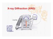
x-ray diffraction
| PowerPoint PPT presentation | free to download
images (insets a, b, c, and d) versus growth time ... Insets are. depiction of quantum structure. formation and TEM cross ... Inset: TEM cross-section of AlN ...
| PowerPoint PPT presentation | free to download
Title: Microsoft PowerPoint Tutorial Author: Clarkson University Last modified by: Saltiel Created Date: 7/25/2001 3:22:57 PM Document presentation format
| PowerPoint PPT presentation | free to download
... Conversion Between Electrons and Photons. Light-emitting diodes (LEDs) (display, lighting, ... Light-Emitting Diodes (LEDs) ... LED lights on an Audi S6. 10. Laser Diodes (LDs) ...
| PowerPoint PPT presentation | free to view
Graphics for single scans, area scans and wafer maps ... Simulation of hexagonal nitride alloy layers with choice of substrate. Modelling of relaxed interfaces ...
| PowerPoint PPT presentation | free to view
Sections 17-1 to 17-5 ... Energy recovery from automobile engines ... Automobile refrigeration. TE combined with fluidics for better heat exchangers ...
| PowerPoint PPT presentation | free to view
ME 381R Lecture 20: Nanostructured Thermoelectric Materials Dr. Li Shi Department of Mechanical Engineering The University of Texas at Austin Austin, TX 78712
| PowerPoint PPT presentation | free to view
Title: Prezentace aplikace PowerPoint Author: fzu Last modified by: vit Created Date: 9/8/2006 9:35:19 AM Document presentation format: P edv d n na obrazovce
| PowerPoint PPT presentation | free to view
Quantum corrected full-band Cellular Monte Carlo simulation of AlGaN/GaN HEMTs ... Calculate the electron density with the new potential (Fermi-Dirac statistics) ...
| PowerPoint PPT presentation | free to download
Synthesize a library of monodisperse functional nanoparticles (NP) ... bis(8-imidazol-1-yloctyl)disulfide. 2. Solution Phase and Nucleation. Fat Fractals ...
| PowerPoint PPT presentation | free to download
If two domains are magnetized in same direction, the bit is a 0 ... Both utilize magnetic data's effect on resistance, but that's the only similarity ...
| PowerPoint PPT presentation | free to download
THIN LAYERS OF TRANSITION METAL OXIDES Tjipke Hibma Materials Science Centre, University of Groningen, The Netherlands Ultimate goal: Epitaxial growth of perfect thin ...
| PowerPoint PPT presentation | free to download
Latest development of InGaN and Short-Wavelength LD/LED/VCSEL Man-lin Tu Introduction Using shorter wavelength blue lasers would decrease the spot size on ...
| PowerPoint PPT presentation | free to download
MATERIALS SCIENCE & ENGINEERING SUBLATTICES & SUBCRYSTALS Part of A Learner s Guide AN INTRODUCTORY E-BOOK Anandh Subramaniam & Kantesh Balani
| PowerPoint PPT presentation | free to download
Materials Science and Engineering Aspects of Nanostructures and Nanomaterials Gottlieb S. Oehrlein Department of Materials & Nuclear Engineering
| PowerPoint PPT presentation | free to download
About Omics Group OMICS Group International through its Open Access Initiative is committed to make genuine and reliable contributions to the scientific community.
| PowerPoint PPT presentation | free to view
Recent Advances in Magneto-Optics Katsuaki Sato Department of Applied Physics Tokyo University of Agriculture & Technology CONTENTS Introduction Fundamentals of ...
| PowerPoint PPT presentation | free to download
As a result, the center of electronic charge at each atomic site is displaced ... Boris Yakobson, Rice University. Ramanan Krishnamoorti. University of Houston ...
| PowerPoint PPT presentation | free to download
III. Applications: iii) Ternary alloys. Stoichiometric composition X2YZ ... iii) Ternary systems. iv) Layered structures. Clean V(001), Cr(001) and Fe (100) surfaces ...
| PowerPoint PPT presentation | free to view
... Conversion Between Electrons and Photons. Light-emitting diodes (LEDs) (display, lighting, ... Light-Emitting Diodes (LEDs) ... LED lights on an Audi S6. 11. Laser Diodes (LDs) ...
| PowerPoint PPT presentation | free to view
Euler began looking at integrals as solutions to differential equations in the ... Finally, in 1785, Laplace began using a transformation to solve equations of ...
| PowerPoint PPT presentation | free to view
Ultra-low Thermal Conductivity of Layered Crystals. Pawel Keblinski, ... Alumina. copper. diamond. YSZ. Phonons Phonons electrons Phonons = 1/3 c v ...
| PowerPoint PPT presentation | free to view
Tunable Terahertz Metamaterials
| PowerPoint PPT presentation | free to download
energy band diagrams modeling. Cornell University: W.J. Schaff and Hai Lu. InN growth, re-growth. ... Also nonlinear polarization relationship was used ...
| PowerPoint PPT presentation | free to view
Novel Periodic Solid State Devices for. Terahertz Emission and Detection ... InSb or Si composite bolometer to detect emission (left) ...
| PowerPoint PPT presentation | free to download
National School on Neutron and XRay Scattering
| PowerPoint PPT presentation | free to view
Faculty of Science. Physics Department ... Theory of Condensed Matter Physics: (Bose-Einsten condensation, Quantum field theory) ...
| PowerPoint PPT presentation | free to download
Friedrich-Schiller-Universit t Jena. Germany. Optical absorption. 0. 2. 4. 6. 8. 10. 12. 14 ... a-plane on a-plane GaN/AlN. on r-plane sapphire (MBE) ...
| PowerPoint PPT presentation | free to view
Summary of different tools for post-processing and visualization ... SIESTA, single-zeta polarized basis. total. Fe, d. DENCHAR. PLRHO. DOS and PDOS. total. Fe, d ...
| PowerPoint PPT presentation | free to download
Hila Hashemi, University of California, Berkeley. Jinquan Xu, Mentor, Florida State University ... Bird RB, Stewart WE, and Lightfoot EN, Transfer Phenomena, ...
| PowerPoint PPT presentation | free to download
(Rosenbaum, Jaeger) (Guyot-Sionnest) April 7, 2003. UC-ANL ... of surface plasmon. field intensity. topography. transmission. Scherer / Wiederecht / Jaeger ...
| PowerPoint PPT presentation | free to view


