Status of Layer 0 - PowerPoint PPT Presentation
1 / 8
Title:
Status of Layer 0
Description:
Also a proposal of the location of conductive area of p and n ... looks like satiation, but why at such low current? Low pass filter and HV prototype ... – PowerPoint PPT presentation
Number of Views:33
Avg rating:3.0/5.0
Title: Status of Layer 0
1
Status of Layer 0
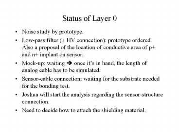
- Noise study by prototype.
- Low-pass filter ( HV connection) prototype
ordered. Also a proposal of the location of
conductive area of p and n implant on sensor. - Mock-up waiting ? once its in hand, the length
of analog cable has to be simulated. - Sensor-cable connection waiting for the
substrate needed for the bonding test. - Joshua will start the analysis regarding the
sensor-structure connection. - Need to decide how to attach the shielding
material.
2
Noise with bias (44V)
expected internal noise 490 50C(pF)e
2000e ( C(sensor) 10pF, C(cable) 20pF,
series noise is 400e ) ? 2 ADC counts
total noise
common mode subtracted
3
Total noise without bias
bias current changed by light shielding.
0 nA
20 nA
4 mA
? looks like satiation, but why at such low
current?
4
Low pass filter and HV prototype
3 mm
resistance 0603 (1.6 x 0.81 x 0.9 mm)
spacer for wire bonding
capacitor 1210 (2.5 x 3.2 x 1.27 mm)
15.5 mm
12 mm
GND
HV
substrate under cables
8 mm
Al foil to back plane (2mm width)
5
Connection to the sensor
4 mm
3mm
15.5 mm
p (GND)
n (HV)
6
Sensor cable connection
7
HV connection to the backplane
side view
Al foil
sensor
kapton insulator
electrically non-conductive glue
electrically conductive glue
thermally conductive material ? need choice
bottom view
16.5 mm
5 mm
5 mm
3 mm
2 mm
8
Shielding connection at hybrid
???


