
Switching circuits - PowerPoint PPT Presentation
1 / 42
Title:
Switching circuits
Description:
Switching circuits. Composed of switching elements called 'gates' that ... Push bubbles to obtain cancellations. Push bubbles to obtain cancellations. Conclude: ... – PowerPoint PPT presentation
Number of Views:117
Avg rating:3.0/5.0
Title: Switching circuits
1
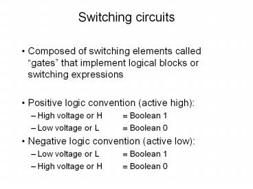
Switching circuits
- Composed of switching elements called gates
that implement logical blocks or switching
expressions - Positive logic convention (active high)
- High voltage or H ? Boolean 1
- Low voltage or L ? Boolean 0
- Negative logic convention (active low)
- Low voltage or L ? Boolean 1
- High voltage or H ? Boolean 0
2
Switching circuits
- Logic variables ? inputs/outputs ? signals
- Signals asserted when the voltage level assumes
the corresponding 1 value - Positive logic asserted by H
- Negative logic asserted by L
- Logic variables are written complemented when
they are active low - Active high signals a, b, c
- Active low signals a, e, u
3
Logic gates
- Logic gates ? switching functions
- Gate symbols two sets
4
Logic gates
- Gate symbols two sets
5
Logic gates
- The NAND logic function and gate
6
Logic gates
- The NAND gate can be used to implement all 3
elementary operations of switching algebra AND,
OR, NOT
7
Logic gates
- The set AND, OR, NOT implements any switching
function (by definition) it is functionally
complete - Therefore, the NAND gate can be used to
implement any switching function - It is functionally complete, or primitive
8
Logic gates
- The NOR logic function and gate
9
Logic gates
- The NOR function can be used to implement all 3
elementary operations of switching algebra AND,
OR, NOT - It is functionally complete too
10
Logic gates
- The NOR logic function and gate
11
Logic gates and equivalence
- CMOS is inverting logic
- NOR and NAND are easier to implement than OR and
AND - They are implemented as NOR or NAND followed by
an inverter - More than one representation is possible for the
same switching function - Different circuits of logic gates might perform
the same switching function - Simpler networks are preferable
- Need to analyze for equivalence and transform
12
Logic gates and equivalence
- Equivalent logic networks
13
Logic gates and equivalence
- Proving the equivalence
14
Digital circuits
- Analysis
- Given a circuit, abstract the Boolean function it
is implementing and try to improve the
implementation or verify the function - From gate diagrams
- From timing diagrams
- Synthesis
- Given a switching function, obtain the
corresponding switching network
15
Analysis
- Timing diagram
16
Analysis
- Truth table
17
Analysis
- Switching network
18
Combinational analysis
19
Signal expressions
- Multiply outF ((X Y) Z) (X Y Z)
(X Z) (Y Z) (X Y Z)
20
New circuit, same function
21
Any number of manipulations can yield equivalent
circuits e.g.
F ((X Y)Z) XYZ Note XYZZ 0
(X Y)XYZ 0 (XYZ)(XYZ)
XYZ So, F (X Y) XYZZ XYZ
(X Y X)(X Y Y)(X Y Z)(Z
X)(Z Y)(Z Z) (1)(1)(X Y
Z)(X Z)(Y Z)(1) (X Y Z)(X
Z)(Y Z) Circuit
22
Push bubbles to obtain cancellations
23
Push bubbles to obtain cancellations
24
Conclude given circuit gt many equivalent
equations circuit does not determine equation
25
Also, equation does not determine circuit
26
Combinational analysis given circuit, determine
function Combinational synthesis given
function, determine circuit
27
Prime number detector F ? (1, 2, 3, 5, 7, 11,
13) AND-OR design
28
Alarm
Derive truth table or expand A P E ? EX ?
(W ? D ? G) P E ? EX ? (W D G) P
E ? EX ? W E ? EX ? D E ? EX ? G
29
A P E ? EX ? W E ? EX ? D E ? EX ?
G
30
NANDs, NORs have fewer transistors than ANDs,
ORs AND-OR converts readily to NAND-NAND
31
Complication if some inputs go directly to second
stage
32
OR-AND to NOR-NOR
33
Bubble-pushing produces non-standard
gate Solution inverters
34
Bubble-pushing produces non-standard
gate Solution inverters
35
Bubble-pushing produces non-standard
gate Solution inverters
36
Propagation delay
37
Propagation delay
38
39
Synthesis
- SOP functions -gt AND OR networks
- POS functions -gt OR AND networks
- Not always possible to design directly
- Fan-in and out restrictions
- Most designs are modular and multi-level
- Modern designs are too complex
- Design and testing by computers
- VLSI - CAD
40
(No Transcript)
41
Logic simulation
- Two states only for an ideal logic signal
- Two gates driving the same line in opposite
directions - Input left not connected or floating
- Third state X is added to the set of states
- Truth tables change
42
Synthesis approaches illustrated to this point
Truth table derivation of minterms Ad hoc
construction of logic equation Need systematic
approach that minimizes hardware Karnaugh
maps Quine-McCluskey algorithm