APh9a - PowerPoint PPT Presentation
1 / 67
Title: APh9a
1
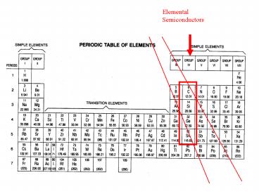
Elemental Semiconductors
2
Insulator Semiconductor Metal
3
5x10²² atoms/cm3 in Si 5x10²² orbitals/band
(Pauli exclusion principle limits 1e/orbital),
But in Si, there are only 1.5x10¹⁰ e/cm3
Electron gas in a metal like gold 6x10²² e/cm3
mobile electrons.
4
Diamond Crystal Structure
5
Energy of orbital
8.6x10⁻⁵ eV/K
Probability of full orbital Probability of empty
orbital
exp(E-EF)/kT
2.718
Chemical potential
6
Direct vs. indirect bandgap semi-conductors
7
k 8.6x10⁻⁵ eV/K
kT 0.0259 eV at 300K
q 1.6x10⁻¹⁹ C
Youll need this soon!
Wavelength (micrometer) 1.24/energy (eV)
8
(No Transcript)
9
Tetrahedral arrangement
10
Statistically, there are always some electrons
which will have enough thermal energy to escape
the valence band (used for covalent bonding) and
can move through the lattice to conduct electric
current
11
Intrinsic Semiconductor case
The slope of the ln(conductivity) vs 1/T plot can
be used to extract the bandgap (Eg/2k) for an
undoped semiconductor
??oexp(-Eg/kT)
Higher Temperature leads to higher conductivity
12
Photoconduction and Photoluminescence
Absorption Detector current in a photoconductor
Luminescence Light emitting diode and lasers
13
It Io exp(?l)
detector
Io
It
Sample with thickness l
14
E 1.24/lambda
Si Eg 1.1 eV wavelength 1060 nm
GaAs Eg
Ge Eg
Si Eg
15
Radiative and Non-radiative recombination in
semiconductors
16
The electro-magnetic spectrum in semiconductor
terms
17
LED materials and spectra
18
Eye response curve and overlap with red LED source
19
(No Transcript)
20
(No Transcript)
21
(No Transcript)
22
Total internal reflection the largest
efficiency problem of LEDs
23
(No Transcript)
24
(No Transcript)
25
(No Transcript)
26
Opto-isolators with diodes and detectors
27
Light emitting diodes for telecommunications.
28
(No Transcript)
29
(No Transcript)
30
(No Transcript)
31
(No Transcript)
32
(No Transcript)
33
(No Transcript)
34
(No Transcript)
35
(No Transcript)
36
(No Transcript)
37
(No Transcript)
38
(No Transcript)
39
(No Transcript)
40
(No Transcript)
41
(No Transcript)
42
(No Transcript)
43
Plasmon-assisted OLEDs?
44
(No Transcript)
45
(No Transcript)
46
(No Transcript)
47
(No Transcript)
48
(No Transcript)
49
(No Transcript)
50
Plasmon Resonances in Metals
51
Light localization vs. light extraction
52
Application High Efficiency Surface Plasmon LED
- Build a light emitting device with
- High efficiency
- Large spontaneous emission enhancement
- High modulation speed
- Explore surface plasmon bandstructure and
different ways of using metals at optical
frequencies
53
Total Internal Reflection
17? escape cone
For normal light emitting diodes with
semiconductor refractive index of 3, the external
efficiency is limited due to total internal
reflection at the semiconductor/air surface.
54
Surface plasmons
?2 lt0
--- --- ---
?1gt 0
- bad nonradiative
- good large density of states
- (spontaneous emission enhancement)
- bad penetration depth into semiconductor lt20nm
55
Quantum well close to a single metal mirror
- Modulation speed of a quantum well can be
increased from 0.8 GHz to 1.4 GHz - Output intensity decreased by factor of 10.
- Dennis Deppe et al., Elect. Lett., 26, 1990
(experimental) - Dennis Deppe et al., IEEE Journal Quant. Elect.
29, 1993 (theoretical)
56
Photonic crystal structures for efficient light
extraction
- Motivation build an efficient LED
- increase extraction efficiency
- increase spontaneous emission rate
- increase modulation speed
- improve directionality
- use electrical contact as light extractor
57
Experimental Measurement Geometry
58
Influence of Type of Metal on InGaN
PL spectra of InGaN/GaN QWs coated with Ag, Al
and Au. The distance between the metal layers and
QWs was 10 nm. The PL peak intensity of uncoated
InGaN/GaN QW (black line) at 470 nm was
normalized to 1.
59
Plasmon Energies of Different Metals
Dispersion diagram of surface plasmon generated
on Ag/GaN (red line), Al/GaN (blue line) and
Au/GaN (green line) surfaces. The dotted line is
the PL spectrum of InGaN/GaN.
60
Influence of Distance between Metal and InGaN QW
Spacer thickness and Excitation power
dependence. a. The PL enhancement ratios were
measured for samples with Ag (red square), Al
(blue triangle), and Au (green circle) plotted
against the thicknesses of GaN spacers.
61
Temperature dependent efficiency
0
10
Data shows that the plasmon enhancement is a
result of improvements of both internal quantum
efficiency as well as external quantum efficiency
Ag Al no metal
1.0
PL Integrated Intensity (a.u.)
-1
0.8
10
PL Integrated Intensity (a.u.)
0.4
0.2
0.0
100
200
300
Temperature (K)
-2
10
0
10
20
30
40
50
1000/T (K-1)
62
Streak Camera Results
Without metal With metal
63
Influence of Metal on Surface
64
Fabrication procedure
65
Grating coupler and a band diagram of SP on
gratings
?
?
kph
1
?1
2
kx
?2
ksp
a
?
1
kx
?/a
66
TE modes in metallic photonic crystals
E
25 nm Ag 90 nm GaAs 200 nm Ag
?x ? 33
67
Measurement results
TM
TETM
- 46x PL enhancement
- wafers with periodicities
- of 480nm and 650nm
- have spectra similar to
- unpatterned structure (c)


