
Barrier dynamics effects on electron transmission through molecular wires and layers PowerPoint PPT Presentation
Title: Barrier dynamics effects on electron transmission through molecular wires and layers
1
Barrier dynamics effects on electron transmission
through molecular wires and layers
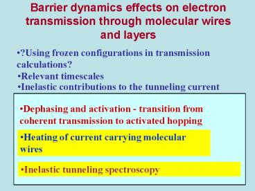
- ?Using frozen configurations in transmission
calculations?
- Relevant timescales
- Inelastic contributions to the tunneling current
- Dephasing and activation - transition from
coherent transmission to activated hopping
- Heating of current carrying molecular wires
- Inelastic tunneling spectroscopy
2
Heating in current carrying molecular
junctions Dvira Segal and AN, J. Chem.
Phys., 117, 3915 (2002)
Thermal conductance through molecular wires Dvira
Segal, AN and P. Hänggi, J. Chem. Phys. 119,
6840 (2003)
Inelastic tunneling spectroscopy Peaks and dips
Michael Galperin, M.A. Ratner and AN
3
Elastic transmission vs. maximum heat generation
??
4
Heating
5
The quantum heat flux
Transmission coefficient at frequency w
With Dvira Segal and Peter Hanggi
6
Anharmonicity effects
Heat current vs. chain length from classical
simulations. Full line harmonic chain dashed
line anharmonic chain using the alkane force
field parameters dash-dotted line anharmonic
chain with unphysically large (x 30) anharmonicity
7
Heat conduction in alkanes of different chain
length
The thermal conductance vs. the chain length for
Alkanes, ?c400 cm-1 , VLVR50 cm-2.
Black T50K Red T300K Blue
T1000K
?c400 cm-1 , VLVR200 cm-2. Black T50K
Red T300K Blue T1000K.
8
Inelastic tunneling spectroscopy Peaks and dips
With Michael Galperin and Mark Ratner
9
Localization of Inelastic Tunneling and the
Determination of Atomic-Scale Structure with
Chemical Specificity B.C.Stipe, M.A.Rezaei and W.
Ho, PRL, 82, 1724 (1999)
STM image (a) and single-molecule vibrational
spectra (b) of three acetylene isotopes on
Cu(100) at 8 K. The vibrational spectra on
Ni(100)are shown in (c). The imaged area in (a),
56Å x 56Å, was scanned at 50 mV sample bias and
1nA tunneling current
Recall van Ruitenbeek et al (Pt/H2)- dips
10
Electronic Resonance and Symmetry in
Single-Molecule Inelastic Electron
TunnelingJ.R.Hahn,H.J.Lee,and W.Ho, PRL 85,
1914 (2000)
Single molecule vibrational spectra obtained by
STM-IETS for 16O2 (curve a),18O2 (curve b), and
the clean Ag(110)surface (curve c).The O2 spectra
were taken over a position 1.6 Å from the
molecular center along the 001 axis. The
feature at 82.0 (76.6)meV for 16O2 (18O2) is
assigned to the O-O stretch vibration, in close
agreement with the values of 80 meV for 16O2
obtained by EELS. The symmetric O2 -Ag stretch
(30 meV for 16O2) was not observed.The
vibrational feature at 38.3 (35.8)meV for 16O2
(18O2)is attributed to the antisymmetric O2
-Ag stretch vibration.
11
Inelastic Electron Tunneling Spectroscopy
ofAlkanedithiol Self-Assembled Monolayers W.
Wang, T. Lee, I. Kretzschmar and M. A. Reed
(Yale, 2004)
Inelastic electron tunneling spectra of C8
dithiol SAM obtained from lock-in second harmonic
measurements with an AC modulation of 8.7 mV (RMS
value) at a frequency of 503 Hz (T 4.2 K).Peaks
labeled are most probably background due to the
encasing Si3N4
Nano letters, in press
12
Raman Scattering
incident
scattered
13
INELSTIC ELECTRON TUNNELING SPECTROSCOPY
14
Nanomechanical oscillations in a single C60
transistorH. Park, J. Park, A.K.L. Lim, E.H.
Anderson, A. P. Alivisatos and P. L. McEuen
NATURE, 407, 57 (2000)
Vsd(mV)
Two-dimensional differential conductance
(?I/?V)plots as a function of the bias voltage
(V) and the gate voltage (Vg ). The dark
triangular regions correspond to the conductance
gap, and the bright lines represent peaks in the
differential conductance.
Vg(Volt)
15
Conductance of Small Molecular JunctionsN.B.Zhite
nev, H.Meng and Z.BaoPRL 88, 226801 (2002)
38mV 22 125 35,45,24
Conductance of the T3 sample as a function of
source-drain bias at T 4.2 K. The steps in
conductance are spaced by 22 mV. Left inset
conductance vs source-drain bias curves taken at
different temperatures for the T3 sample (the
room temperature curve is not shown because of
large switching noise). Right inset
differential conductance vs source-drain bias
measured for two different T3 samples at T 4.2
K.
16
MODEL
17
Parameters
GL
GR
electrons
e1
M
Molecular vibrations
w0
U
Thermal environment
M from reorganization energy (M2/w0) U from
vibrational relaxation rates
18
NEGF
( anticommutator)
19
A1
A2M
A3M2
elastic
inelastic
elastic
20
(No Transcript)
21
(No Transcript)
22
Changing position of molecular resonance
23
Changing tip-molecule distance
24
IETS (intrinsic?) linewidth
GL
GR
electrons
e1
M
Molecular vibrations
w0
U
Thermal environment
M from reorganization energy (M2/w0) U from
vibrational relaxation rates
25
IETS linewidth
e11eV GL0.5eV GR0.05eV w00.13eV M2/w00.7eV
26
Conclusions
- IETS Peaks or dips in 2nd I/V derivative and
their shapes depend on parametrs. In
particular, the position of the electronic
resonance and its coupling to an STM lead can be
controlled. - While perturbation theory can qualitatively
predict such results, it may fail quantitatively
in a way that impact the qualitative observation
It may predict peaks instead of dips and it
misses overtones. - Satellite peaks may be observed in 1st I/V
derivative if electronic resonance is narrow
enough. - Intrinsic linewidth in IETS may be due to
broadening of phonon peaks due to coupling to
metal electrons
27
Satellite peaks
28
Inelastic Electron Tunneling Spectroscopy
ofAlkanedithiol Self-Assembled Monolayers W.
Wang, T. Lee, I. Kretzschmar and M. A. Reed
(Yale, 2004)
Inelastic electron tunneling spectra of C8
dithiol SAM obtained from lock-in second harmonic
measurements with an AC modulation of 8.7 mV (RMS
value) at a frequency of 503 Hz (T 4.2 K).Peaks
labeled are most probably background due to the
encasing Si3N4
Nano letters, in press
Recommended
