0. Deposit film of interest onto substrate. PowerPoint PPT Presentation
Title: 0. Deposit film of interest onto substrate.
1
Patterning using Photolithography Pattern
Transfer by Etching
All the patterns (devices features) to make the
transistors are made using the photolithographic
process.
0. Deposit film of interest onto substrate.
2. Softbake photoresist to dry it.
3. Align photomask to wafer features.
4. Expose photoresist through mask.
5. Develop photoresist.
6. Etch film using resist as a mask.
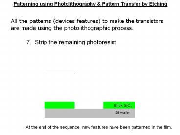
7. Strip the remaining photoresist.
1. Spin photoresist onto wafer.
thick SiO2
Si wafer
At the end of the sequence, new features have
been patterned in the film.
PowerShow.com is a leading presentation sharing website. It has millions of presentations already uploaded and available with 1,000s more being uploaded by its users every day. Whatever your area of interest, here you’ll be able to find and view presentations you’ll love and possibly download. And, best of all, it is completely free and easy to use.
You might even have a presentation you’d like to share with others. If so, just upload it to PowerShow.com. We’ll convert it to an HTML5 slideshow that includes all the media types you’ve already added: audio, video, music, pictures, animations and transition effects. Then you can share it with your target audience as well as PowerShow.com’s millions of monthly visitors. And, again, it’s all free.
About the Developers
PowerShow.com is brought to you by CrystalGraphics, the award-winning developer and market-leading publisher of rich-media enhancement products for presentations. Our product offerings include millions of PowerPoint templates, diagrams, animated 3D characters and more.

