
Soft Lithographic Patterning of EMI Shields onto Concave Missile Domes PowerPoint PPT Presentation
1 / 1
Title: Soft Lithographic Patterning of EMI Shields onto Concave Missile Domes
1
Soft Lithographic Patterning of EMI Shields onto
Concave Missile Domes
To shield sensitive missile systems against
Electromagnetic Interference (EMI), the concave
dome of a missile can be decorated with a square
metallic grid consisting of open spaces about
1/25th as wide as the wavelength of the target
radiation. Grid lines must also be about 1 mil or
less in width to avoid obscuring the infrared
view through the dome. Most techniques for
defining micro-scale features, such as e-beam
writing, standard photolithography, and ink jet
printing, are not readily suitable for use on
non-flat surfaces. The current method of
decorating domes with a fine grid illustrates the
problem. First, the metal (usually gold) is vapor
deposited onto the inside surface of the dome.
The desired pattern is then written directly on
the surface in photoresist using a laser writing
process the writing alone requires about an hour
of processing time. Finally, the dome is dipped
into an etch bath, leaving only the metal defined
by the photoresist pattern. This process results
in a grid that is elongated near the edges of the
dome. Furthermore, the method serially produces
decorated domes in a labor and equipment
intensive process. A cost-effective and rapid
method (preferably one that does not use
expensive equipment in the final fabrication of
the decorated domes) is needed to mass produce
missiles with advanced shielding and sensing
capabilities. Economical EMI shielding that will
create minimal interference with useful radiation
will benefit military systems beyond missiles,
such as ubiquitous sensors, spacecraft and
aircraft.
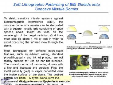
Illustration showing the process of Soft
Lithographic micro-contact printing (mCP) to
pattern the insides of missile domes.
Example of soft lithographic patterning of curved
surfaces. The metal ball bearings (left) were
decorated with 500nmdiameter circles with around
100nm line widths (right).
Brian T. Mayers, Nano-Terra Inc., Work performed
at Center for Nanoscale Systems -Harvard
Recommended
