Methods PowerPoint PPT Presentation
1 / 25
Title: Methods
1
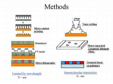
Methods
10nm
Nano-writing
Micro-contact printing
Monolayer
Phase separated Langmuir-Blodgett Films
UV mask
Oriented block co-polymers
Micro-lithography
Intermolecular interaction X nm
Limited by wavelength X ?m
2
Island Surfaces are Formed By Using SAMs with Two
Different Functional Groups
Chemical Functionalities Differing in size and
type Examples CH3-, NH2-, CF3-, COOH-, halide,
ethylene oxide
matrix
Nanoisland
3
Recessed Islands of APhMS In OTS Background by
Backfilling
OTS
?m
P-Aminophenyltrimethoxy silane
8 Å
Temp 220C
Silicon wafer
4
Recessed Islands of APhMS In OTS Background by
Backfilling
OTS
?m
octadecyltrichlorosilane
Temp 220C
Ht difference 15 Å
5
Method B Co-Adsorption
OTS
APhMS
CH3
amine
30nm
23Å
6.5Å
Silicon wafer
Mixed monolayer of OTS and APS(NH2C3H6SiCl3)
P-aminophenyltrimethoxysilanes (APhMS)
octadecyltrichlorosilanes (OTS)
6
Island Formation of Co-Adsorbed Self-assembling
Surfactants
APhMS islands in OTS Matrix
35 islands/µm2, average diameter 28
nm, distribution width 10 nm
31 OTSAPhMS Chloroform 2mM total concentration
of silane
7
Effect of Composition
2 mM CHCl3 solution, deposition time 2 hrs
OTS/APMS11 OTS Pillars
OTS/APMS13 OTS Pillars
OTS/APMS31 APhMS islands
8
Solvent Effect
2 mM solution (OTS/APhMS11), deposition time 2
hrs,
Toluene
CHCl3
Contact Angles 103
Contact Angles 98
CCl4
THF
Contact Angles 80
Contact Angles 41
9
Effect of Solvent on Composition
- Monolayer Composition in Mixed Adsorption is a
balance between - relative affinity of surfactants to the
depositing solvent - interfacial energy between the film formed
and the depositing solution
10
Sequential Adsorption for Mixed Monolayers
Rinse
Partial OTS monolayers with desired islands Low
density surrounding OTS islands at100C.
Fill surrounding with second silane
11
Temperature Effect
100C
Reduced Secondary growth at low temperatures
220C
12
Control of Morphology and Chemical Functionality
at Nanometer Scale
10?
2?
Height
Friction
Friction
Height
30nm to 10 µm
Br
CH3
23Å
15Å
Silicon wafer
Mixed monolayer of OTS and BrUTS(BrC11H22SiCl3)
13
Control of Morphology at Angstrom Scale
10?
Height
Friction
Mixed monolayer of OTS and DTS(C10H21SiCl3)
14
Nano-dots
5?
Low OTS concentration low deposition time
15
pH 8. . .
Imaging at loads of 1.5 GPa (70 nN). . . 3
scans
unworn
unworn
worn
. . . leads to rapid pit formation and facile
dissolution
16
pH 5. . . Imaging at loads of 0.7 GPa (58 nN).
. .10 scans
17
pH 5. . . Imaging at loads of 1.6 GPa (96 nN).
. . 10 scans
. . . charging followed by surface atom
abstraction is observed
18
pH 3. . . Imaging at loads of 0.7 GPa (56 nN).
. .83 scans!
. . . no wear to be found, even with increased
loads! . . . no charging due to low OH-.
19
Studies of Lubricant Films Functionalization of
AFM tip and Particle Surface
AFM Tip
Functionalization with organosilanes
CH3(CH2)17-Si(OCH2CH3)3 (OTE)
- Forms self-assembled monolayers on silica. -
Have been used in MEMS devices.
Contact angle with water on OTE modified
particle films
Si(100)
20
Thiols on Au
Salmeron and Liu
21
Nanopatterning of Surfaces
22
AFM
STM
23
C18S/Au
C18S implanted in a C10S/Au
Liu et al, Acc. Chem. Res. 33 (2000) 457.
24
Mirkin dip-pen lithography
Allows fab in air!
Amro et al, Langmuir 16 (2000) 3006.
25
(No Transcript)

