WP2.2 Slab Data Paths PowerPoint PPT Presentation
Title: WP2.2 Slab Data Paths
1
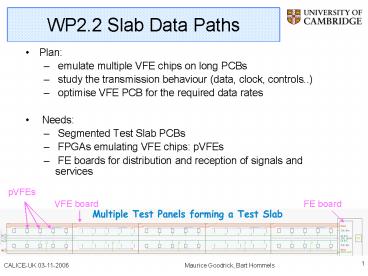
WP2.2 Slab Data Paths
- Plan
- emulate multiple VFE chips on long PCBs
- study the transmission behaviour (data, clock,
controls..) - optimise VFE PCB for the required data rates
- Needs
- Segmented Test Slab PCBs
- FPGAs emulating VFE chips pVFEs
- FE boards for distribution and reception of
signals and services
pVFEs
VFE board
FE board
2
VFE PCB progress
- Features thin (64mum) layers and narrow (75mum)
traces - Traces for various clock distr. schemes and/or
readout architectures - Rows of 4 FPGAs/board
- Every FPGA mimics 2 VFE chips
- Board schematics are finished
- PCB layout completed
3
FPGA Firmware for VFE emulation
- official VHDL code obtained from VFE chip
designers at LAL (thanks!) - VHDL code adapted for FPGA synthesis
- testbench for pVFE in VHDL
4
Evaluation board for tests
- Purchased Xilinx - Digilent evaluation board
- Spartan 3E FPGA suits our tests many output
standards and speeds supported - Versatile test system 32MB SRAM, RS232, USB,
Ethernet 10/100, user connectors, etc. - Excellent price/performance
5
pVFE simulation
- Synthesized VFE VHDL code using Xilinx coregen
RAM - Two pVFEstestbenches running on evaluation board
(X3S500E device) - Design fits into envisaged pVFE FPGA and yet
leaves room for extras - 25 of logic used
- 83 of block RAM used.
- Preliminary code available for alternative pVFE
implementation
6
High data rate alternative
- Low output data rate relies on effective
zero-suppression - Assumed low noise and low occupancy
- If assumptions prove wrong, much higher data
rates are to be expected - Investigate high-rate capability of slab data path
- ATLC/SPICE simulation of fast signals over PCB
traces - Spartan3E supports output rates of 200MHz
7
pVFE firmware current status
- Preliminary system in place,
- Data Generator
- pVFE controller
- Serial transmission (by DHCAL emulator)
- Receiver
- Next step
- system capable of
- Bit Error Rate Testing
- Data are stored in RAM
- Initial data are compared with data sent through
serial transmission chain
8
Outlook and plans
- Manufacture VFE PCB panels (very) soon
- Define FE board requirements and interface
- Continue firmware development for pVFE and FE
- Think of interface with outside world
PowerShow.com is a leading presentation sharing website. It has millions of presentations already uploaded and available with 1,000s more being uploaded by its users every day. Whatever your area of interest, here you’ll be able to find and view presentations you’ll love and possibly download. And, best of all, it is completely free and easy to use.
You might even have a presentation you’d like to share with others. If so, just upload it to PowerShow.com. We’ll convert it to an HTML5 slideshow that includes all the media types you’ve already added: audio, video, music, pictures, animations and transition effects. Then you can share it with your target audience as well as PowerShow.com’s millions of monthly visitors. And, again, it’s all free.
About the Developers
PowerShow.com is brought to you by CrystalGraphics, the award-winning developer and market-leading publisher of rich-media enhancement products for presentations. Our product offerings include millions of PowerPoint templates, diagrams, animated 3D characters and more.

