
A Direct Digital Synthesis DDS AudioRF Signal Generator 1Hz to 30MHz PowerPoint PPT Presentation
1 / 38
Title: A Direct Digital Synthesis DDS AudioRF Signal Generator 1Hz to 30MHz
1
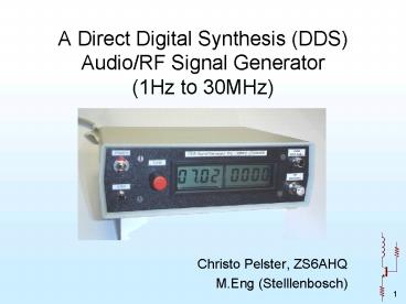
A Direct Digital Synthesis (DDS) Audio/RF Signal
Generator(1Hz to 30MHz)
- Christo Pelster, ZS6AHQ
- M.Eng (Stelllenbosch)
2
Older Versions
They are very useful, but have some shortfalls
- Variable FrequencyOscillators (VFO)
- Free running
- Harmonics are usedfor higher bands
- Frequency not accurate
- Low resolution
- Unknown level/impedance
- Stability and drift problems
- Availability where to buy
3
Newer Versions
Professional Equipment is VERY expensive You get
what you pay for, but few amateurs can afford the
luxury.
4
Main Design Objectives
- Wide frequency coverage
- Constant and known output levels
- Known output impedance
- Ease of calibration without special test
equipment - Good Frequency accuracy
- Fine tuning resolution
- Good Frequency Stability
- Intermediate construction skills needed to build
- Affordable
- Mixed Analog (Audio, RF) and Digital Design
- Provide a useful tool to the home constructor
5
Main Features
- Output Frequency 1Hz to 30MHz
- Frequency Resolution 1Hz
- Audio Section with 600O impedance from 1Hz to
100kHz - RF Section with 50O impedance from 100kHz to
30MHz - Output level RF0dBm 1.5dB, Audio 0dBm
- Calibrated by using a standard Digital Volt Meter
(DVM) - Easy one button, one knob operation
- Selectable frequency step size
- Large, easily readable 8 digit display
- Pure Sine wave generated by Direct Digital
Synthesis (DDS)
6
Applications
- RF
- Home construction of RF front ends,mixers, IF
amplifiers. - Check frequency readouts andradios with VFO
dials - Frequency reference for VFO transceivers
- S-meter characterization and comparison
- Antenna return loss measurements(requires return
loss bridge)
- Audio
- Audio amplifier frequency response
- Test Sound card frequency responsefor Software
Defined Radios (SDRs)
7
Block Diagram
4 Digit LCD
4 Digit LCD
RotaryEncoder
32
32
LCD_LOAD
AY-043832 segmentLCD Driver
AY-043832 segmentLCD Driver
LCD_DATA
PIC16F628A
LCD_CLK
STEP
SPARE
DDS_CLOCK
DS_FSYNC
DDS_DATA
30MHz
OPA843
OPA843
X-TalRef Osc
50O
RF Out
75MHz
LPF
RF OP Amp
RF OP Amp
5V
-5V
Vref
600O
Power Supply
Audio Out
MC33172Audio OP Amp
230VAC
8
Functional Description (1)
- Display Function
- Man-Machine Interface
- 4-digit LCDs with 7-segment displays
- Displays the generated frequency with 1Hz
resolution
- Frequency Control Function
- Rotary Encoder that can be turned
- Push button to select step size
- Blinked digit indicate which step size is selected
9
Functional Description (2)
- Control Function (what the PIC does)
- Check frequency limits and set limits when
reached - Check Step Change input and change the step size
if the push button switch has been pressed - Check for changes in the Rotary Encoder
(increment or decrement) - Calculate and look up the 7 segment values of the
digits and send them to the display - Calculate the DDS word and send it to the DDS IC
(Not multi-tasking, but all these tasks are done
between every detentof the rotary encoder, so
fast that the user does not even notice)
10
Functional Description (3)
- Analogue Audio Section
- 1st Audio Op Amp buffers DDS reference signal.
- 2nd Audio Op Amp inverts, amplifies and
subtract VREF. - Drives 600O output (0dBm and -60dBm)
- Analogue RF Section
- 1st RF Op Amp buffers DDS output and drives Low
Pass Filter (LPF). Sets gain DC coupled. - LPF removes DDS harmonics
- 2nd RF Op Amp AC coupled output stage (0dBm)
drives 50O (0dBm) - -73dBm attenuator for S-9 measurements
11
Analogue Section Circuit Diagram
12
Theory of Operation (1)
DDS How does a Direct Digital Synthesizer
generate a signal
The phase angle (?) rotates througha fixed angle
for each unit of time
13
Theory of Operation (2)
The AD9834 builds the output based on this
equation.
14
Theory of Operation (2)
The angular rate depends on the Frequency of the
signal
? 2pf
Knowing that the phase of a sine wave is linear
and given a reference interval (clock period),
the phase rotation for that period can be
determined.
?Phase ? ?t
? ?Phase / ?t 2pf
Solving for f and substituting the reference
clock frequency for the reference period (1/fMCLK
?t)
f ?Phase fMCLK/2p
The AD9834 builds the output based on this
equation.
15
Theory of Operation (3)
AD9834 Block Diagram (from Analog Devices data
sheet).
16
Theory of Operation (4)
Audio Section Op Amp Differential
Configuration.
FromDDS output(VDDS)
Output 0VDC 4.4Vp-p
-Vss
FromDDS VREF
17
Theory of Operation (5)
- Audio Section
- Two Equations with 4 unknowns..! (VREF 1.2V)
- Solve iteratively by first assuming RF 10 x RG
- Calculate R1, R2 for 0V DC offset (assume R12k2)
- Adjust gain to 10.5, re-calc R2 for 0V DC offset
etc - R12k2, R23k9, RF18.8k (12k6k8), RG1k8
- Try to keep R1R2 RFRG (approx 1.4 to 1.6k)
18
Theory of Operation (6)
Output Voltage from DDS 0.42Vp-p with DC offset
FSD Value 18 x (VREF/RSET) x RDDS
19
Theory of Operation (7)
Inverting Amplifier m -RF/RG 10.5 for 0dBm
in 600O
-4.4V is equal to 4.4Vp-p
20
Theory of Operation (8)
Add Offset b2.1 DC offset is now 0V
4.4Vp-p0VDC
21
Theory of Operation (9)
2.1Vp-p(loaded)
4.4Vp-p(unloaded)
PL (dBm) 10 x LOG(PL x 1000) 0dBm
22
Theory of Operation (10)
RF Section RF Op Amps Inverting Configuration.
FromDDS output(IFSD)
Output VDDS 0.421Vp-p
IFSD3.18mAR1(eff) 133O
Output 0.655Vp-p
23
Theory of Operation (11)
RF Section Low Pass Filter 5th order
Elliptical 0.1dB Passband Ripple Standard
Component Values L1, L2 11 turns, 24AWG on 4mm
drill bit tightly wound
24
Theory of Operation (12)
Cut off at 30MHz, Stop Band at 45MHz
25
Theory of Operation (13)
RF Section Final Gain Stage DC Block, 0dBm
210mVRMS(0.6Vp-p)
FromLPF output
Output 1.28Vp-p(Unloaded)
Compensation for LPF gain roll-off
26
Theory of Operation (14)
0.64Vp-p(loaded)
1.28Vp-p(unloaded)
PL (dBm) 10 x LOG(PL x 1000) 0dBm
27
Results (1) RF Output Level
Amplitude dBm
Frequency MHz
28
Results (2) 30MHz
Amplitude dBm
Frequency MHz
29
Results (3) Audio M0KGK SDR
Amplitude dBm
Frequency Hz
30
Construction
- 4 PCB Boards
- Display Board
- Analogue Board
- Power Supply Board
- -73dBm Attenuator Board
- 3 Components only available in Surface Mount
- 1 x DDS IC AD9834CRUZ
- 2 x RF OP Amps OPA843ID
- 1 x 75MHz Clock Oscillator
31
Display Board
- 2 x 4-digit displays placed side-by-side in
sockets - 2 x AY-0438 32 segment shift registers LCD
drivers - Easy to read, 12.7mm high digits
- Fast response vs. 2 x 16 display controllers
- Good contrast
- Rotary Encoder 24 pulses/rev. 4 pulses/detent
- Double sided PCB
32
Analogue Board
- PIC Micro Controller 16F628A - Microchip
- DDS IC AD9834CRUZ Analog Devices
- 75MHz Clock Oscillator - Crystek
- RF OP Amps OPA843IP Texas Instruments
- Audio OP Amp MC33172P On-Semi
- 3.3V Regulator MCP1702 - Microchip
- Discrete Resistors, Inductors, Capacitors
- Double Sided PCB
33
Power Supply
- Power Supply 5V (500mA) and -5V (100mA)
- 6-0-6V 1.5VA PCB mount transformer
- Single Sided PCB
34
-73dBm Attenuator
- 3 x 20dB 1 x 13dB Stages
- Zin 50R with -38dB RL
- Zout 50R with -29dB RL
- Double Sided PCB
35
Assembled Unit front view
36
Assembled Unit rear view
37
Availability
- Double Sided Through-hole plated PCB with Solder
Mask and Silk Screen in progress. - Depending on the interest, kits (excl. enclosure)
with SMD components already mounted can be
compiled. - Provide Name, Call sign and e-mail address on
inquiry form.
38
The Audio/RF DDS Signal Generatoris a handy
addition to the shack of any home constructor of
radio equipment
- Thank you
- Christo Pelster, ZS6AHQ
Recommended
