
IO devices - PowerPoint PPT Presentation
1 / 25
Title:
IO devices
Description:
Peripheral devices (also called I/O devices) are pieces of equipment that ... and springiness with low damping they will be 'bouncy' as they make and break. ... – PowerPoint PPT presentation
Number of Views:29
Avg rating:3.0/5.0
Title: IO devices
1
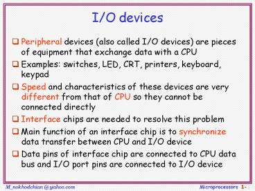
I/O devices
- Peripheral devices (also called I/O devices) are
pieces of equipment that exchange data with a CPU - Examples switches, LED, CRT, printers, keyboard,
keypad - Speed and characteristics of these devices are
very different from that of CPU so they cannot be
connected directly - Interface chips are needed to resolve this
problem - Main function of an interface chip is to
synchronize data transfer between CPU and I/O
device - Data pins of interface chip are connected to CPU
data bus and I/O port pins are connected to I/O
device
2
I/O devices
- Since a CPU may have multiple I/O devices, CPU
data bus may be connected to data buses of
multiple interface - An address decoder is used to select one device
to respond to the CPU I/O request - Different CPUs deal with I/O devices differently
- Some CPUs have dedicated instructions for
performing input and output operations (isolated
I/O) - Other CPUs use the same instruction for reading
from memory and reading from input devices, as
well as writing data into memory and writing data
into output devices (memory-mapped I/O) - MCS-51 (8051) is memory mapped
3
Synchronization of CPU and interface chip
- There must be a mechanism to make sure that there
are valid data in the interface chip when CPU
reads them - Input synchronization two ways of doing this
- Polling method
- interface chip uses a status bit to indicate if
it has valid data for CPU - CPU keeps checking status bit until it is set,
and then reads data from interface chip - Simple method, used when CPU has nothing else to
do - Interrupt driven method interface chip
interrupts the CPU when it has new data. CPU
executes the ISR
4
Synchronization of CPU and interface chip
- Output synchronization two ways of doing this
- Polling method
- interface chip uses a status bit to indicate that
the data register is empty - CPU keeps checking status bit until it is set,
and then writes data into interface chip - Interrupt driven method interface chip
interrupts the CPU when it data register is
empty. CPU executes the ISR
5
Synchronization of CPU and interface chip
- Methods used to synchronize data transfer between
interface chip and I/O devices - Brute force method interface chip returns
voltage levels in its input ports to CPU and
makes data written by CPU directly available on
its output ports - All 8051 port can perform brute force I/O
- Strobe method
- During input, the I/O device activates a strobe
signal when data are stable. Interface chip
latches the data - For output, interface chip places output data on
output port. when data is stable, it activates a
strobe signal. I/O device latches the data - Handshake method two handshake signals are
needed - One is asserted by interface chip and the other
by I/O device
6
8051 ports
7
8051 ports
- Ports 1, 2, and 3 have internal pullups, and Port
0 has open drain outputs. - To be used as an input, the port bit latch must
contain a 1, which turns off the output driver
FET. - For Ports 1, 2, and 3, the pin is pulled high by
a weak internal pullup, and can be pulled low by
an external source. - Port 0 differs in that its internal pullups are
not active during normal port operation (writing
a 1 to the bit latch leaves both output FETs off,
so the pin floats).
8
8051 I/O Ports Hardware Specs
- P0 is open drain.
- Has to be pulled high by external 10K resistors.
- Not needed if P0 is used for address lines
- P1, P2, P3 have internal pull-ups
- Port fan- out (number of devices it can drive) is
limited. - Use buffers (74LS244, 74LS245,etc) to increase
drive. - P1, P2, P3 can drive up to 4 LS-TTL inputs
9
8051 - Switch On I/O Ports
- Case-1
- Gives a logic 0 on switch close
- Current is 0.5ma on switch close
- Case-2
- Gives a logic 1 on switch close
- High current on switch close
- Case-3
- Can damage port if 0 is output
10
Simple input devices
- DIP switches usually have 8 switches
- Use the case-1 from previous page
- Sequence of instructions to read a value from DIP
switches - mov P1,FFH
- mov A,P1,
11
Interfacing a Keypad
- A 16-key keypad is built as shown in the figure
below. - 16 keys arranged as a 4X4 matrix.
- Must activate each row by placing a 0 on its
R output. - Then the column output is read.
- If there is a 0 on one of the column bits, then
the button at the column/row intersection has
been pressed. - Otherwise, try next row.
- Repeat constantly
12
Bouncing Contacts
- Push-button switches, toggle switches, and
electromechanical relays all have one thing in
common contacts. - Metal contacts make and break the circuit and
carry the current in switches and relays. Because
they are metal, contacts have mass. - Since at least one of the contacts is movable, it
has springiness. - Since contacts are designed to open and close
quickly, there is little resistance (damping) to
their movement
13
Bouncing
- Because the moving contacts have mass and
springiness with low damping they will be
"bouncy" as they make and break. - That is, when a normally open (N.O.) pair of
contacts is closed, the contacts will come
together and bounce off each other several times
before finally coming to rest in a closed
position. - The effect is called "contact bounce" or, in a
switch, "switch bounce.
14
Why is it a problem?
- If such a switch is used as a source to an
edge-triggered input such as INT0, then the
MCS-51 will think that there were several
events and respond several times. - The bouncing of the switch may last for several
milliseconds. - Given that the MCS-51 operates at microsecond
speed, a short ISR may execute several times in
response to the above described bounciness
15
Hardware Solution
- The simplest hardware solution uses an RC time
constant to suppress the bounce. The time
constant has to be larger than the switch bounce
and is typically 0.1 seconds. - As long as capacitor voltage does not exceed a
threshold value, the output signal will be
continued to be recognized as a logic 1. - The buffer after the switch produces a sharp
high-to-low transition.
16
Hardware Solution
17
Software Solution
- It is also possible to counter the bouncing
problem using software. - The easies way is the wait-and-see technique
- When the input drops, an appropriate delay is
executed (10 ms), then the value of the line is
checked again to make sure the line has stopped
bouncing
18
Interfacing a Keypad
- scan mov P1,EFH
- jnb P1.0,db_0
- scan1 jnb P1.1,db_1
- scan2 jnb P1.2,db_2
- scan3 jnb P1.3,db_3
- scan4 mov P1,DFH
- jnb P1.0,db_4
- ..
- ..
- ..
8051
D
E
F
C
9
A
B
8
5
6
7
4
0
1
2
3
19
Interfacing a Keypad
- db_0 lcall wt_10ms
- jb P1.0, scan1
- mov A, 0
- ljmp get_code
- db_1 lcall wt_10ms
- jb P1.1, scan2
- mov A, 1
- ljmp get_code
- ..
- ..
- get_code mov DPRT, key_tab
- movc A, _at_ADPRT
- ljmp scan
- key_tab db 0123456789ABCDEF
- END
20
Simple output devices
- Case-1
- LED is ON for an output of zero
- Most LEDs drop 1.7 to 2.5 volts and need about
10ma - Current is (5-2)/470
- Case-2
- Too much current
- Failure of Port or LED
- Case-3
- Not enough drive (1ma)
- LED too dim
21
The 7-Segment Display
- 7 LEDs arranged to form the number 8.
- By turning on and off the appropriate segments
(LEDs), different combinations can be roduced. - useful for displaying the digits 0 through 9,
and some characters.
22
The 7-segment Display (Cont.)
- 7-segment displays come in 2 configurations
- Common Anode Common Cathode
- As we have seen, it would be preferable to
connect the cathode of each diode to the output
pin. - Therefore, the common anode variety would be
better for our interfacing needs.
23
Interfacing a 7-segment display
- Also, as seen with interfacing the LED, a
resistor will be needed to control the current
flowing through the diode. - This leaves two possibilities
- Case 2 would be more appropriate as case 1 will
produce different brightness depending on the
number of LEDs turned on.
24
Use of current buffer
- Interfacing to a DIP switch and 7-segment display
- Output a 1 to ON a segment
- We can use 74244 to common cathode 7_seg
25
BCD to 7_Seg lookup table
- mov a,p3
- anl a,0fh
- get_code mov DPTR, 7s_tab
- movc A, _at_ADPRT
- mov p1,a
- 7s_tab db 3fh,30h,5bh,4fh,66h
- db 6dh,7dh,07h,7fh,6fh
- END
a
a
a
a
a
a
a
a
f
b
b
b
f
b
f
f
f
b
b
f
b
f
g
g
g
g
g
g
g
e
e
c
c
c
e
c
c
e
c
c
e
c
d
d
d
d
d
d
d
Recommended
CrystalGraphics Presentations


