Instrumentation for High Energy Particle and Nuclear Physics PowerPoint PPT Presentation
Title: Instrumentation for High Energy Particle and Nuclear Physics
1
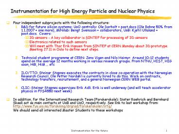
Instrumentation for High Energy Particle and
Nuclear Physics
- Four independent subprojects with the following
structure - RD for future silicon systems UoO centrally
Ole Dorholt post.docs (Ole Rohne 50 from
1.1.2007 one more), MiNilab Bengt Svensson
collaborators, UoB Kjetil Ullaland post.docs.
Covers - 3D sensors - A key collaborator is SINTEF for
processing of 3D sensors - Electronics related to such sensors
- Will meet with Thor Erik Hansen from SINTEF at
CERN Monday about 3D prototype. Meeting 27.11 in
Oslo to define next steps. - Techncial student programme at CERN Jens Vigen
and Nils Hoimyr. Around 10-12 students spend on
the average 12 months working in various research
groups. From NTNU, HIST, HIG soon, HiB, HiM etc - ILO/TTO Steinar Stapnes executes the contracts
in close co-operation with the Norwegian Research
Council. Ole Petter Nordahl is currently hired to
do this. Work on contracts, technology transfers,
recruitement, and a general Norwegian CERN WEB
portal. - CLIC Steinar Stapnes supervises Erik Adli. Erik
is well underway (and will teach accelerator
physics in FYS4550 next week) - In addition, for the International Research Team
(Forskerskole) Dieter Roehrich and Bernhard
Skaali act as main contacts at UoB and UoO,
respectively. See link to last workshop from
http//www.fys.uio.no/forskning/drgrad/forskerskol
er/irtg/ - We should send all interested Master Students to
these workshops
2
Schematics of 3D- and ordinary detector structures
- Proposed by S.I. Parker, C.J. Kenney and J.
Segal (NIM A 395 (1997) 328) - Called 3-D because, in contrast to silicon
planar technology, have three dimensional (3-D)
electrodes penetrating the silicon substrate - SINTEF/UiO are currently processing 3D
structures for a group consisting investigation
by a collaboration within Brunel Univ., Hawaii
Univ., Stanford Univ. and CERN
-
depletion thickness depends on p and n
electrode distance, not on the substrate
thickness ? (1) can operate at very low voltages,
(2) can have a high doping for ultra-high
radiation hardness, (3) are fast and (4) can be
active almost to the edge
PowerShow.com is a leading presentation sharing website. It has millions of presentations already uploaded and available with 1,000s more being uploaded by its users every day. Whatever your area of interest, here you’ll be able to find and view presentations you’ll love and possibly download. And, best of all, it is completely free and easy to use.
You might even have a presentation you’d like to share with others. If so, just upload it to PowerShow.com. We’ll convert it to an HTML5 slideshow that includes all the media types you’ve already added: audio, video, music, pictures, animations and transition effects. Then you can share it with your target audience as well as PowerShow.com’s millions of monthly visitors. And, again, it’s all free.
About the Developers
PowerShow.com is brought to you by CrystalGraphics, the award-winning developer and market-leading publisher of rich-media enhancement products for presentations. Our product offerings include millions of PowerPoint templates, diagrams, animated 3D characters and more.

