LVDS%20Tx/Rx%20for%20DSS PowerPoint PPT Presentation
Title: LVDS%20Tx/Rx%20for%20DSS
1
LVDS Tx/Rx for DSS
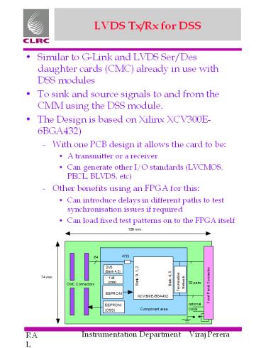
- Similar to G-Link and LVDS Ser/Des daughter
cards (CMC) already in use with DSS modules - To sink and source signals to and from the CMM
using the DSS module. - The Design is based on Xilinx XCV300E-6BGA432)
- With one PCB design it allows the card to be
- A transmitter or a receiver
- Can generate other I/O standards (LVCMOS, PECL,
BLVDS, etc) - Other benefits using an FPGA for this
- Can introduce delays in different paths to test
synchronisation issues if required - Can load fixed test patterns on to the FPGA itself
2
LVDS Tx/Rx for DSS
- Status
- Specification at http//www.te.rl.ac.uk/esdg/atlas
-flt/ under DSS daughter cards - Schematics completed and awaiting PCB layout
PowerShow.com is a leading presentation sharing website. It has millions of presentations already uploaded and available with 1,000s more being uploaded by its users every day. Whatever your area of interest, here you’ll be able to find and view presentations you’ll love and possibly download. And, best of all, it is completely free and easy to use.
You might even have a presentation you’d like to share with others. If so, just upload it to PowerShow.com. We’ll convert it to an HTML5 slideshow that includes all the media types you’ve already added: audio, video, music, pictures, animations and transition effects. Then you can share it with your target audience as well as PowerShow.com’s millions of monthly visitors. And, again, it’s all free.
About the Developers
PowerShow.com is brought to you by CrystalGraphics, the award-winning developer and market-leading publisher of rich-media enhancement products for presentations. Our product offerings include millions of PowerPoint templates, diagrams, animated 3D characters and more.

