IEEE2005 PowerPoint PPT Presentation
1 / 1
Title: IEEE2005
1
A Novel CMOS Monolithic Active Pixel Sensor with
Analog Signal Processing and 100 Fill
factor J.P. Crooks3, J.A. Ballin1, P.D.
Dauncey1,A-M. Magnan1, Y. Mikami2, O. Miller2,M.
Noy1, V. Rajovic2, M. Stanitzki3, K.D. Stefanov3,
R. Turchetta3, M. Tyndel3, E.GiulioVillani3, N.
K. Watson2, J. A. Wilson2 1Imperial College
London, 2University of Birmingham, 3 STFC
Rutherford Appleton Laboratory
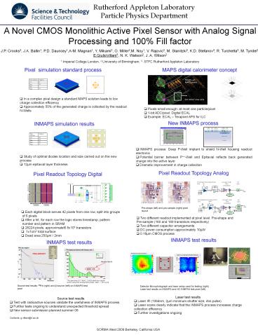
Pixel simulation standard process
MAPS digital calorimeter concept
Pixel collection Charge (e-)
ltQgt 87
Qmax 362
Qmin1 5
Qstdev 107
50?50 µm2 MAPS pixels
- In a complex pixel design a standard MAPS
solution leads to low charge collection
efficiency - Approximately 50 of the generated charge is
collected by the readout N-Wells
SiD 16mm2 area cells
- Pixels small enough at most one particle/pixel
- 1-bit ADC/pixel Digital ECAL
- Example ECAL Terapixel APS for ILC
New INMAPS process
INMAPS simulation results
Pixel collection Charge (e-)
ltQgt 401
Qmax 656
Qmin1 261
Qstdev 95
- INMAPS process Deep P-Well implant to shield
N-Well housing readout electronic - Potential barrier between P-Well and Epitaxial
reflects back generated charge into the active
layer - Dramatic improvement in charge collection
- Study of optimal diodes location and size
carried out on the new process - 12µm epitaxial layer thickness
Pixel Readout Topology Analog
Pixel Readout Topology Digital
- Each digital block serves 42 pixels from one
row, split into groups of 6 pixels - After a hit, for each row the logic stores
timestamp, pattern number and pattern in SRAM - 28224 pixels, approximatel6 8x10⁶ transistors
- 1x1cm2 total surface
- Dead area 250µm / 2mm
Pre-shape (left) and pre-sample (right) pixel
layout
- Two different readout implemented at pixel
level Pre-shape andPre-sample (160 and 189
transistors respectively) - Two different capacitor arrangements
- DC power consumption approximately 10µW
- 0.18µm CMOS process
INMAPS test results
INMAPS test results
Detector Microphotograph and laser setup used for
testing (right). Laser test results on INMAPS and
NO INMPAS test pixel (left).
Source test results 55Fe (right) and ß source
(left) on INMAPS test pixel
- Laser test results
- Laser IR (1064nm, 2µm minimum shutter size, 4ns
pulse) - Laser scans clearly indicate that the INMAPS
process increases charge collection efficiency - Further investigations ongoing
- Source test results
- Test with radioactive sources validate the
usefulness of INMAPS process - Further tests ongoing to understand unexpected
threshold spread - New sensor submission planned summer 08
Contacts g.villani_at_rl.ac.uk
SORMA West 2008 Berkeley, California USA

