Motivation PowerPoint PPT Presentation
1 / 1
Title: Motivation
1
Scanning Tunneling Microscopy of GaCrN Grown by
MBE Muhammad B. Haider1, Rong Yang1, Costel
Constantin1, Erdong Lu1, Hamad Al-Brithen1, David
Ingram1, ArthurR.Smith1,Gabriel Caruntu2, and
Charles J. OConnor2. 1Condensed Matter and
Surface Science, Department of Physics and
Astronomy, Ohio University, Athens, OH 45701 2
Advanced Materials Research Intitute, University
of New Orleans, New Orleans, LA 70148
- Motivation
- Dilute Magnetic semiconductors(DMS) are very
important for Spintronics application - Sato et al. have predicted GaCrN to be a DMS with
Tc above room temperature if CrGa bulk ratio is
above 2. - Goals
- To investigate GaCrN growth under different
growth conditions to find the conditions where Cr
substitutes Ga lattice site and 2nd phases are
not formed. - To perform STM studies to confirm the position
and behavior of Cr in GaN(000i) lattice on the
atomic level.
Abstract According to Sato et al. (Ga,Cr)N is
expected to show ferromagnetic behavior above
room temperature if the bulk CrGa concentration
is above 2.1Although many techniques (mainly
bulk) have been applied to study dilute magnetic
nitride semiconductor systems here we apply in
situ STM to investigate the issues of Cr
incorporation and Cr diffusion/segregation.
Cr-doped GaN(000i) has been grown using
rf-plasma molecular beam epitaxy (MBE) on
Sapphire (0001) at sample temperature of
approximately 700 oC. The Ga/N flux ratio has
been varied from 65-100 with variable Cr/Ga
flux ratio set between 3-11 for GaCrN growth.
Based on the Ga/N flux ratio, three growth
regimes were found N-rich, metal-rich and
Ga-rich. It was found that under all three
conditions GaCrN surfaces are smoother even to
atomistic level forming 3 ? 3 reconstructions
after the growth as revealed by RHEED and AFM.
Atomic scale STM images of Ga-rich GaN(000i)
covered with 0.05 mono-layer (ML) of Cr show 3 ?
3 and 6 ? 6 reconstructions indicating the
presence of Cr atoms within the surface
structure. STM images of GaCrN surface with Cr/Ga
flux ratio of 20 and above show some linear
features suggesting transition from Cr
substitution to 2nd phase nucleation at the
surface. The 3 ? 3 reconstruction has been
observed by RHEED and STM upon exposure of Cr to
GaN(000i) 1 ? 1 at room temperature. These STM
images suggest that on GaCrN surface, at low Cr
concentration, Cr occupies Ga surface position.
1- Sato et al. J. Superconduc, 16 (2003) 31
STM studies of Cr doped GaN(000i)
SQUID and XRD measurement of Ga-rich GaCrN sample
RHEED and STM image of Cr on 1 ? 1 GaN (000i)
surface
N-Polar GaN Surface
Experiment 6ML of GaCrN with Cr/Ga flux ratio of
5 and Ts700 oC
Inverted Contrast
N-Polar GaCrN surface
RHEED and AFM images of Bulk GaCrN
- ZFC/FC measurements as a function of temperature.
- Hysteresis measurement at 5K and 300K show
ferromagnetic behavior of the Ga-rich GaCrN
sample - XRD does not show any 2nd phases.
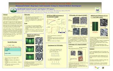
- Cr seem to incorporate in GaN lattice. Bright
features in the 3 ? 3 reconstruction correspond
to Cr atoms - 6 ? 6 reconstruction of GaCrN seems like
contrast reversal effect of regular 6 ? 6
reconstruction of GaN which could be due to
unintentional Cr coating of the STM tip.
- Cr formed 3x3 reconstruction when deposited at RT
on GaN 1x1 surface. This is evident from the
RHEED scan and STM image. - STM image shown above contain 3x3
reconstructions which is an anti-corrugation of
regular GaN 3x3 reconstruction which is again due
to some Cr atoms sticking on the tip. - Moreover there are some bright features on the
surface, which are probably some impurity
adsorbates on the surface.
Growth Procedure
STM images of Cr doped GaN(000i) Experiment 4ML
of Ga-rich GaCrN with Cr/Ga flux ratio of 20 at
Ts 700 oC
Experiments for STM Studies
Ga, N and Cr atoms
GaCrN(000i)
- Summary
- Cr has a smoothening effect on GaCrN growth, even
under N-rich conditions growth is smoother than
N-rich GaN growth. - GaCrN growth under Ga-rich conditions and Cr/Ga
flux ratio less than 3 results in smooth single
phase growth. - STM study reveals that Cr substitutes Ga lattice
sites on the surface if Cr/Ga flux ratio is lt 5. - At higher Cr/Ga flux ratios, Cr starts
precipitating along high symmetry lines forming
Cr nano-wires.
- 3-6 ML of GaCrN deposited on Ga-rich GaN(000i) at
700 oC with 5 and 20 Cr/Ga flux ratio
Cr in GaN Cr/Ga flux ratio 5
Cr in GaN Cr/Ga flux ratio 20
GaN(000i)
Sapphire (0001)
It .08nA Vs 1.3V
It .08nA Vs -1V
- Solvent Cleaning of the Sapphire (0001) substrate
- Heating and Nitridation of the substrate at
Ts800 oC - GaN buffer layer growth thickness 200nm, Ts
700 oC - GaCrN growth Ga/N flux ratio 65-110,
- Cr/Ga flux ratio 2-20
Schematic model of GaCrN surface with 20 Cr/Ga
flux ratio
2. 0.09ML of Cr deposition on 1x1 GaN adlayer
at room temperature
- Found three growth regimes of GaCrN growth,
N-rich, metal-rich, and Ga-rich - Cr is acting as surfactant, ie smoothening
effect on the surface. Even N-rich surface has
3?3 reconstructions.
- STM images show the surface solubility limit of
Cr as a function of Cr/Ga flux ratio - Higher concentration of Cr doping results in Cr
segregation on the surface along high symmetry
lines forming Cr nano-wires

