OUTLINE PowerPoint PPT Presentation
1 / 19
Title: OUTLINE
1
Lecture 17
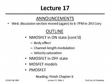
- ANNOUNCEMENTS
- Wed. discussion section moved (again) to 6-7PM in
293 Cory
- OUTLINE
- NMOSFET in ON state (contd)
- Body effect
- Channel-length modulation
- Velocity saturation
- NMOSFET in OFF state
- MOSFET models
- PMOSFET
- Reading Finish Chapter 6
2
The Body Effect
- VTH is increased by reverse-biasing the
body-source PN junction
g is the body effect parameter.
3
Channel-Length Modulation
- The pinch-off point moves toward the source as
VDS increases. - The length of the inversion-layer channel becomes
shorter with increasing VDS. - ID increases (slightly) with increasing VDS in
the saturation region of operation.
l is the channel length modulation coefficient.
4
? and L
- The effect of channel-length modulation is less
for a long-channel MOSFET than for a
short-channel MOSFET.
5
Velocity Saturation
- In state-of-the-art MOSFETs, the channel is very
short (lt0.1mm) hence the lateral electric field
is very high and carrier drift velocities can
reach their saturation levels. - The electric field magnitude at which the carrier
velocity saturates is Esat.
6
Impact of Velocity Saturation
- Recall that
- If VDS gt EsatL, the carrier velocity will
saturate and hence the drain current will
saturate - ID,sat is proportional to VGSVTH rather than
(VGS VTH)2 - ID,sat is not dependent on L
- ID,sat is dependent on W
7
Short-Channel MOSFET ID-VDS
P. Bai et al. (Intel Corp.), Intl Electron
Devices Meeting, 2004.
- ID,sat is proportional to VGS-VTH rather than
(VGS-VTH)2 - VD,sat is smaller than VGS-VTH
- Channel-length modulation is apparent (?)
8
Drain Induced Barrier Lowering (DIBL)
- In a short-channel MOSFET, the source drain
regions each support a significant fraction of
the total channel depletion charge QdepWL - ? VTH is lower than for a long-channel MOSFET
- As the drain voltage increases, the reverse bias
on the body-drain PN junction increases, and
hence the drain depletion region widens. - VTH decreases with increasing drain bias.
- (The barrier to carrier diffusion from the source
into the channel is reduced.) - ? ID increases with increasing drain bias.
9
NMOSFET in OFF State
- We had previously assumed that there is no
channel current when VGS lt VTH. This is
incorrect! - As VGS is reduced (toward 0 V) below VTH, the
potential barrier to carrier diffusion from the
source into the channel is increased. ID
becomes limited by carrier diffusion into the
channel, rather than by carrier drift through the
channel. - (This is similar to the case of a PN junction
diode!) - ID varies exponentially with the potential
barrier height at the source, which varies
directly with the channel potential.
10
Sub-Threshold Leakage Current
- Recall that, in the depletion (sub-threshold)
region of operation, the channel potential is
capacitively coupled to the gate potential. A
change in gate voltage (DVGS) results in a change
in channel voltage (DVCS) - Therefore, the sub-threshold current (ID,subth)
decreases exponentially with linearly decreasing
VGS/m
log (ID)
ID
Sub-threshold swing
VGS
VGS
11
Short-Channel MOSFET ID-VGS
P. Bai et al. (Intel Corp.), Intl Electron
Devices Meeting, 2004.
12
VTH Design Trade-Off
- Low VTH is desirable for high ON-state current
- ID,sat ? (VDD - VTH)? 1 lt ? lt 2
- But high VTH is needed for low OFF-state current
log ID
Low VTH
- VTH cannot be reduced aggressively.
High VTH
IOFF,low VTH
IOFF,high VTH
VGS
0
13
MOSFET Large-Signal Models (VGS gt VTH)
- Depending on the value of VDS, the MOSFET can be
represented with different large-signal models.
VDS ltlt 2(VGS-VTH)
VDS lt VD,sat
VDS gt VD,sat
14
MOSFET Transconductance, gm
- Transconductance (gm) is a measure of how much
the drain current changes when the gate voltage
changes. - For amplifier applications, the MOSFET is usually
operating in the saturation region. - For a long-channel MOSFET
- For a short-channel MOSFET
15
MOSFET Small-Signal Model (Saturation Region of
Operation)
- The effect of channel-length modulation or DIBL
(which cause ID to increase linearly with VDS) is
modeled by the transistor output resistance, ro.
16
PMOS Transistor
- A p-channel MOSFET behaves similarly to an
n-channel MOSFET, except the polarities for ID
and VGS are reversed. - The small-signal model for a PMOSFET is the same
as that for an NMOSFET. - The values of gm and ro will be different for a
PMOSFET vs. an NMOSFET, since mobility
saturation velocity are different for holes vs.
electrons.
Circuit symbol
Schematic cross-section
17
PMOS I-V Equations
- For VDS lt VD,sat
- For VDS gt VD,sat
for long channel
for short channel
18
CMOS Technology
- It possible to form deep n-type regions (well)
within a p-type substrate to allow PMOSFETs and
NMOSFETs to be co-fabricated on a single
substrate. - This is referred to as CMOS (Complementary MOS)
technology.
Schematic cross-section of CMOS devices
19
Comparison of BJT and MOSFET
- The BJT can achieve much higher gm than a MOSFET,
for a given bias current, due to its exponential
I-V characteristic.

