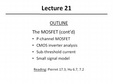
OUTLINE - PowerPoint PPT Presentation
1 / 19
Title:
OUTLINE
Description:
Lecture 21 OUTLINE The MOSFET (cont d) P-channel MOSFET CMOS inverter analysis Sub-threshold current Small signal model Reading: Pierret 17.3; Hu 6.7, 7.2 – PowerPoint PPT presentation
Number of Views:114
Avg rating:3.0/5.0
Title: OUTLINE
1
Lecture 21
- OUTLINE
- The MOSFET (contd)
- P-channel MOSFET
- CMOS inverter analysis
- Sub-threshold current
- Small signal model
- Reading Pierret 17.3 Hu 6.7, 7.2
2
P-Channel MOSFET
- The PMOSFET turns on when VGS lt VT
- Holes flow from SOURCE to DRAIN
- ? DRAIN is biased at a lower potential than the
SOURCE - In a CMOS technology, the PMOS NMOS threshold
voltages are usually symmetric about 0, i.e. VTp
-VTn
VG
- VDS lt 0
- IDS lt 0
- IDS increases with
- VGS - VT
- VDS (linear region)
VS
VD
GATE
ID
P
P
N
VB
EE130/230M Spring 2013
Lecture 21, Slide 2
3
Long-Channel PMOSFET I-V
- Linear region
- Saturation region
m 1 (3Toxe/WT) is the bulk-charge factor
EE130/230M Spring 2013
Lecture 21, Slide 3
4
CMOS Inverter Intuitive Perspective
CIRCUIT
SWITCH MODELS
VDD
VDD
Rp
VOUT 0V
VOUT VDD
Rn
Low static power consumption, since one MOSFET is
always off in steady state
VIN VDD
VIN 0V
EE130/230M Spring 2013
Lecture 21, Slide 4
5
Voltage Transfer Characteristic
N sat P sat
VOUT
N off P lin
C
VDD
N sat P lin
B
D
E
A
N lin P sat
N lin P off
0
VIN
VDD
0
EE130/230M Spring 2013
Lecture 21, Slide 5
6
CMOS Inverter Load-Line Analysis
VGSpVIN-VDD
VIN VDD VGSp
VDSpVOUT-VDD
VOUT VDD VDSp
IDn-IDp
VIN 0 V
VIN VDD
IDn-IDp
increasing VIN
VOUTVDSn
0
VDD
0
EE130/230M Spring 2013
Lecture 21, Slide 6
7
Load-Line Analysis Region A
VGSpVIN-VDD
VDSpVOUT-VDD
IDn-IDp
VIN ? VTn
IDn-IDp
VOUTVDSn
0
VDD
0
EE130/230M Spring 2013
Lecture 21, Slide 7
8
Load-Line Analysis Region B
VGSpVIN-VDD
VDSpVOUT-VDD
IDn-IDp
IDn-IDp
VDD/2 gt VIN gt VTn
VOUTVDSn
0
VDD
0
EE130/230M Spring 2013
Lecture 21, Slide 8
9
Load-Line Analysis Region D
VGSpVIN-VDD
VDSpVOUT-VDD
IDn-IDp
IDn-IDp
VDD VTp gt VIN gt VDD/2
VOUTVDSn
0
VDD
0
EE130/230M Spring 2013
Lecture 21, Slide 9
10
Load-Line Analysis Region E
VGSpVIN-VDD
VDSpVOUT-VDD
IDn-IDp
VIN gt VDD VTp
IDn-IDp
VOUTVDSn
0
VDD
0
EE130/230M Spring 2013
Lecture 21, Slide 10
11
MOSFET Effective Drive Current, IEFF
M. H. Na et al., IEDM Technical Digest, pp.
121-124, 2002
VIN VDD
NMOS DRAIN CURRENT
VIN ½VDD
VDD
0.5VDD
NMOS DRAIN VOLTAGE VOUT
EE130/230M Spring 2013
Lecture 21, Slide 11
12
Propagation Delay, td
VDD
CMOS inverter chain
Voltage waveforms
VDD
td is reduced by increasing IEFF and reducing
load capacitance C
EE130/230M Spring 2013
Lecture 21, Slide 12
13
Sub-Threshold Current
- For VG lt VT, MOSFET current flow is limited
by carrier diffusion into the channel region. - The electric potential in the channel region
varies linearly with VG, according to the
capacitive voltage divider formula - As the potential barrier to diffusion increases
linearly with decreasing VG, the diffusion
current decreases exponentially
EE130/230M Spring 2013
Lecture 21, Slide 13
14
Sub-Threshold Swing, S
EE130/230M Spring 2013
Lecture 21, Slide 14
15
VT Design Trade-off
- Low VT is desirable for high ON current
- IDsat ? (VDD - VT)? 1 lt ? lt 2
- But high VT is needed for low OFF current
log ID
Low VT
- VT cannot be aggressively reduced!
High VT
IOFF,low VT
IOFF,high VT
VGS
0
EE130/230M Spring 2013
Lecture 21, Slide 15
16
How to minimize S?
EE130/230M Spring 2013
Lecture 21, Slide 16
17
MOSFET Small Signal Model
- Conductance parameters
A small change in VG or VDS will result in a
small change in ID
low-frequency
high-frequency
EE130/230M Spring 2013
Lecture 21, Slide 17
18
Parasitic Components
EE130/230M Spring 2013
Lecture 21, Slide 18
19
MOSFET Cutoff Frequency, fT
The cut-off frequency fT is defined as the
frequency when the current gain is reduced to 1.
vG here is ac signal CG is approximately equal
to the gate capacitance, ? W L Cox
input current
output current
At the cutoff frequency (wT 2pfT)
- Higher MOSFET operating frequency is achieved by
decreasing the channel length L
EE130/230M Spring 2013
Lecture 21, Slide 19


![[PDF] DOWNLOAD FREE Clinical Outline of Oral Pathology: Diagnosis and PowerPoint PPT Presentation](https://s3.amazonaws.com/images.powershow.com/10076578.th0.jpg?_=20240711025)


![[READ]⚡PDF✔ Black Letter Outline on Contracts (Black Letter Outlines) 5th Edition PowerPoint PPT Presentation](https://s3.amazonaws.com/images.powershow.com/10044064.th0.jpg?_=20240531080)


