
Dopants PowerPoint PPT Presentations
All Time
Recommended

Title: Adolescents sportifs et conduites dopantes Author: Patrick LAURE Last modified by: Patrick Created Date: 1/26/2003 12:28:25 PM Document presentation format
| free to view

Lawrence Berkeley National Laboratory, Berkeley, CA 94720. Supported by US DOE and DOD ... C-plane sapphire. InN. AlN. GaN. edge threading dislocations. Ne ~ 80% NTD ...
| free to view

Single Phase Wurtzite Structure No In Clusters. g = (0002) g ... shows only the wurtzite structure. InN pattern with no evidence of. any secondary phase. ...
| free to view

For gelation. For Peptization. Mn(NO3)2 . 4H2O. 1.88 g (7.5 mmol) ... Gelation with H2O. 7.60 ml (420 mmol) Tetra n-butyl-orthotitanate. 10.21 ml (30 mmol) ...
| free to view

The enthalpy and non-configurational entropy of solution, H and Sn-c, are ... Enthalpy and entropy compete, with entropy dominant. 13 ...
| free to view

Title: PowerPoint Presentation Author: David Cohen Last modified by: David Cohen Created Date: 11/30/2002 5:55:03 AM Document presentation format
| free to view

B2H6, burnt chocolate, sickly sweet odor. Poisonous, flammable, and explosive. N-type dopants ... NH3, pungent, irritating odor, corrosive. Dopants for ...
| free to view
CMOS VLSI Digital Design Overview Physical principles Combinational logic Sequential logic Datapath Memories Trends Dopants Silicon is a semiconductor Pure silicon ...
| free to download

Title: Du DOPAGE aux CONDUITES DOPANTES Author: DDJS Last modified by: savin Created Date: 3/30/2004 8:55:11 PM Document presentation format: Affichage l' cran (4:3)
| free to download

CMOS VLSI Design Digital Design Overview Physical principles Combinational logic Sequential logic Datapath Memories Trends Dopants Silicon is a semiconductor Pure ...
| free to download

... tightly and at the correct temperature, the high Z dopants become hydrogenic ... of High-Z Hydrogenic Ion Lines in. Dense Hot Plasmas, 1977) Stark Difficulties ...
| free to download

NOVEL FUNCTIONALISED DOPANTS FOR MELT PROCESSABLE CONDUCTING POLYANILINE ... Protonation. Plasticisation. Solubilisation. Melt. processability ...
| free to view

DOPING E RECURSOS ERGOG NICOS-1 DOPING E DOPAGEM DOPING a pr pria subst ncia dopante(1889 na Inglaterra) DOPAGEM o uso de uma subst ncia ,com finalidade ...
| free to view

Properties enhanced by dopants (Thallium or Sodium) - CsI(Tl) ... Jimi Hendrix. Krankies. Comfortably mediocre. Artistic Merit (log scale) Arsecockfuck ...
| free to view

Experimentally measured values of dopant ionization energies in silicon are 0. ... So at room temperature we see that virtually all common dopants will ionize. ...
| free to view

... developed a method to map the distribution of dopants within ... 14 nm x 14 nm. Shell. Core. Engaging K-12 Teachers in Teaching and Research of Nanomaterials ...
| free to view

These free electrons and holes came from the dopants. ... Note the dopant ions are fixed and cannot move. These dopant ions then act just like charge built-up ...
| free to view

Dopant-assisted Concentration Enhancement of Substitutional Mn in Si and Ge ... the thermodynamics solubility of magnetic dopants is extremely low. ...
| free to view

ECE 875: Electronic Devices Prof. Virginia Ayres Electrical & Computer Engineering Michigan State University ayresv@msu.edu
| free to download

P-n junction diode and other semiconductor
| free to download

VLSI Design Introduction Introduction Integrated circuits: many transistors on one chip. Very Large Scale Integration (VLSI) Complementary Metal Oxide Semiconductor ...
| free to view

Introduction to CMOS VLSI Design Layout, Fabrication, and Elementary Logic Design Introduction Integrated circuits: many transistors on one chip. Very Large Scale ...
| free to download
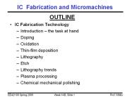
IC Fabrication and Micromachines OUTLINE IC Fabrication Technology Introduction the task at hand Doping Oxidation Thin-film deposition Lithography
| free to download
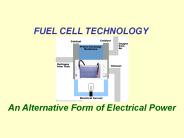
FUEL CELL TECHNOLOGY An Alternative Form of Electrical Power
| free to download
Introduction to CMOS VLSI Design Lecture 0: Introduction David Harris Harvey Mudd College Spring 2004 Administrivia Name Tents Syllabus About the Instructor Office ...
| free to download

Dielectric Properties of Ceramic Thin Films. Mara Howell. Materials Science and Engineering ... Enhanced capacitance is related to original capacitance by the ...
| free to view

Oxidation Content Properties of SiO2 Oxidation Process Functions of SiO2 Equipment for Si Oxidation Mechanism of Si Oxidation Factors affecting oxidation Doping ...
| free to view

Introduction to CMOS VLSI Design Lecture 0: Introduction Credits: David Harris Harvey Mudd College (Material taken/adapted from Harris lecture notes)
| free to download

Title: CMOS Devices : Limitations and Solutions for the End of the Roadmap Author: bf31 Last modified by: Claire Created Date: 5/12/2006 9:26:14 AM
| free to view

Determine if ion implantation damages have any transient effect on diffusion in Ge. Characterization of Si1-xGex formed with Ge/Si intermixing process ...
| free to download


Chu, Gao, and Erickson, J. Vac. Sci. Technol. B, Vol. 16, No. 1, Jan/Feb 1998 Depth Profiles of GaN/InGaN/GaN LED Device . Title: Slide 1 Author:
| free to download

Title: APLICACIONES Author: Carmen Last modified by: User Created Date: 4/28/2006 9:41:14 AM Document presentation format: Presentaci n en pantalla
| free to view

Deal-Grove model (10) - Effect of temperature on the rate constants B, and B/A ... Each of the coefficients B, and B/A has an Arrhenius relationship. of the ...
| free to view
Title: 1.1 Silicon Crystal Structure Author: Blyang Last modified by: tking Created Date: 3/28/2000 4:44:02 PM Document presentation format: On-screen Show
| free to download


Les acteurs de la pr vention et de la lutte contre le dopage ... Les acteurs et leur r le. Le Comit national olympique et sportif fran ais (CNOSF) ...
| free to view

Elemental silicon is melted and grown into a single crystal ingot Single crystal ingot being grown Completed silicon ingot Pure silicon is rarely grown Typically as ...
| free to download

Semiconductor industry is highly interested in viewing dopant profiles at ... We would like to thank Tim Petersen and Vicki Keast for all their input! ...
| free to download

Lecture #3 OUTLINE Band gap energy Density of states Doping Read: Chapter 2 (Section 2.3) Band Gap and Material Classification Measuring Band Gap Energy Density of ...
| free to download

chen,kai. ee40-chentim. chen,timothy_j. ee40-vchen. ee40-chenwuy. chen,wuyang. ... hwang, nicholas jay. samuel, aretha ruth. tahir, muhammad farhan. druzgalski, adrian m.
| free to view
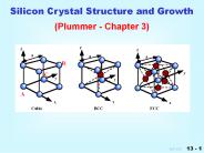
Silicon Crystal Structure and Growth ... mobile electrons tend ... Wafer positioning stage Three-axis piezo substage Figure 7.16 Detector Pinhole ...
| free to download

I have seen this happen ! You have exceeded your storage allocation Creating a n-p junction on a p-type silicon wafer A n-p junction is a diode and a solar cell It ...
| free to download
Title: Molecular Dynamics Author: Chi-Ok Hwang Last modified by: Chi-Ok Hwang Created Date: 5/8/2003 1:10:55 AM Document presentation format:
| free to download

Dopant and Self-Diffusion in Silicon and Silicon Germanium Eugene Haller, Hughes Silvestri, and Chris Liao MS&E, UCB and LBNL FLCC Tutorial 4/18/05
| free to download

Lecture 2 OUTLINE Semiconductor Fundamentals (cont d) Energy band model Band gap energy Density of states Doping Reading: Pierret 2.2-2.3, 3.1.5; Hu 1.3-1.4,1.6, 2.4
| free to view

By Heiner Lichtenberber, Micheal Zasowski, Gery Lovitz & Daniel Ha ... X-ray images. X-ray images were taken of the ICs to show the sweep of the wires. ...
| free to download

2) Fabricaci n de m scaras (b) M scara de dado individual con una ... Exposici n de m scaras y revelado empleando resina fotosensible positiva. 3) Litograf a ...
| free to view

LA CONSULTATION en vue du certificat de non contre indication sportive ASSOCIATION MEDICALE DES MINIMES MEDECINE DU SPORT LE CERTIFICAT DE NON CONTRE INDICATION LE ...
| free to download

International Workshop on a Far Detector in Korea ... Scintillator/Fe Sandwitch. 300 X0 depth ~ 230 Layers. each layer : 15m x 15m. Iron 15m x 15m x 2cm ...
| free to download


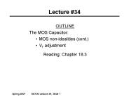
Doping Control is critical in MOS device scaling. ( Scaling down the gate length requires equal scaling in doping profile) Thermal diffusion ...
| free to view

IC Fabrication and ... from a dopant-containing ambient or doped solid source Formation of Insulating Films The favored insulator is pure silicon ...
| free to download

... plasmonics, optical lattice, photonic crystals, and novel quantum effects of light-matter interaction. What have been done on Lithium niobate crystal?
| free to download

CRYSTAL GROWTH, WAFER FABRICATION AND BASIC PROPERTIES OF Si WAFERS- Chapter 3 Crystal Structure Crystals are characterized by a unit cell which repeats in the
| free to view

Silicon electrical properties. 5 * The appearance of Band Gap, separating CB and VB * The 6 CB minima are not located at the center of 1st Brillouin zone, INDIRECT GAP
| free to view