Construction of electronic systems - PowerPoint PPT Presentation
1 / 18
Title:
Construction of electronic systems
Description:
First one used components mounted on isolating cards, connected by soldered connections ... crossing leads problems with single sided boards (can be solved by jumpers) ... – PowerPoint PPT presentation
Number of Views:58
Avg rating:3.0/5.0
Title: Construction of electronic systems
1
Construction of electronic systems C.Bohm Co
mponents
connections 2-pole
(resistors), 3-pole (transistors) 4-pole
(transformers)..10-pole vacuum
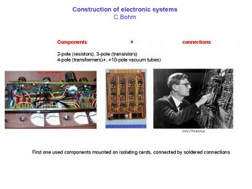
tubes) First one used
components mounted on isolating cards, connected
by soldered connections
John Pinkerton
2
Increased component density demanded other
methods Integrated circuits
single or double
sided circuit boards DIL (dual in line)
packages wire wrapped circuit boards Hole
mounted lt30 legs wrapped circuit boards
printed circuit boards crossing
leads problems with single sided boards (can be
solved by jumpers) You can use vias on
double sided boards (metal deposited holes
usually 0.2-1 mm)
3
LSI (large) ic-circuits
multi layer
boards Large DIL lt100 legs
many routing
layers PGA (pin grid array) better lt350 legs
4
Special power planes supply power to the
components
Long connections have inductance
Active component
Ground bounce
Varying current transport
Nearby decoupling capacitors Deliver charges that
can supply the current transients They work like
energy reservoirs
Power plane with low inductance
Ground plane with low inductance
Ground and power plane have also good shielding
properties
5
Return current
Return current
Low frequent Signal current
High frequent Signal current
Minimize resistance
Minimize inductance
A cut in the ground plane forces the return
current to deviate which affects the signal
quality
A cut in the ground plane can also increase the
cross talk between nearby signals
6
Micro strip
Stripline
Wide trace and small distance gives a
large capacitance difficult to drive
Circuit board materials FR4 (flame retardent
4) Roger (brand name) high speed Poly imide
(Kapton) flexfoïls Rigid flex combination
FR4-Flex foil
7
Multi layer boards allows blind and covered
vias Surface mounting
usually lt 10 layers Higher densities
trace widths gt0.1mm vias gt
0.25mm SO PQFP BGA 28 legs lt400
legs lt600 legs gt0.5 mm/leg gt0.4mm/leg 1.27mm/leg
Thru hole
Usually lt10 layers Trace widthsgt0.1 mm Isolations
distancegt0.1 mm Viasgt0.25 mm dia
blind
covered
Vias through power planes
Via to powerplane
Sufficiently large diameter to match The drill
tolerance
Drop via
Thermal via to simplify soldering
8
micro BGA, CSP lt2000 lt1mm/leg Difficult to
extract the signals between the balls Many
layers are needed Alternative use laser drilled
thin micro via layers which supports very thin
traces
Pictures from elektrotryck.se
9
Laser drilled vias
Pictures from elektrotryck.se
10
From PCBpro.com
Step1 Film Generation Generated from your
design files, we create an exact film
representation of your design. We will create one
film per layer.
Step2 Shear Raw Material Industry standard
0.059" thick, copper clad, two sides. Panels will
be sheared to accommodate many boards.
Step3 Drill Holes Using NC machines and carbide
drills.
Step4 Electroless Copper Apply thin copper
deposit in hole barrels.
11
From PCBpro.com
Step5 Apply Image Apply photosensitive dryfilm
(plate resist) to panel. Use light source and
film to expose panel. Develop selected areas from
panel.
Step6 Pattern Plate Electrochemical process to
build copper in the holes and on the trace area.
Apply tin to surface.
Step7 Strip Etch Remove dryfilm, then etch
exposed copper. The tin protects the copper
circuitry from being etched.
Step8 Solder mask Apply solder mask area to
entire board with the exception of solder pads.
12
From PCBpro.com
Step9 Solder coat Apply solder to pads by
immersing into tank of solder. Hot air knives
level the solder when removed from the tank.
Step10 Nomenclature Apply white letter marking
using screen printing processStep11
Fabrication Route the perimeter of the board
using NC equipment
13
PCB manufacture PCB laminate about 0.2mm
different types FR4, Polyimide (Kapton) and
Roger drill electrolytic plating of
holes connect a voltage source to the two sides
while in a bath add photo resist
illuminate pattern rinse
etch build the layer chemically
glue several layer component print
lack layer test with beds of nails or
flying probes
14
Mounting componentsHole mounting
mount components wave soldering
test Surface mounting solder
mask spread solder paste mount
components (with robot) heat in
oven next side test
15
- Circuit board data
- generate pattern for the different layers
artwork - generate drill files
- Control files to milling machine (to separate and
shape the boards) - Different layers
- Cupper pattern
- Component print
- Lack layer
- Solder mask
- Different physical layers (artwork order)
- 1 signal_1 pad_1
- 2 power_1
- 3 power_2
- signal_2 pad_2
16
Start by creating a schematic Decide board
size shape, silkscreen print, mounting holes,
placing and routing zones Make sure there is a
pattern for each component pads, holes, vias
and component print connect schematic symbols
with legs to component pattern with pads package
circuit board data translate schematics with
symbols to component pattern and net list place
components on the board (side, position,
orientation, ref nr) manual, automatic or
combined draw traces in the connection layer
(with support from schematics) manual,
automatic or combined different trace which
gives different impedances split ground plane
avoid couplings between analogue and digital
parts area fills fill empty areas with
grounded cupper surfaces
17
Soldering Soldering in solder
oven Temperature profile Solder
quality Inferior wetting depend on poor
heating or insufficient amount of flux Lead free
solder enforced in industry higher
temperatures Conductive glue is sometimes an
alternative
Double sided mounting difficult
OK
Not enough solder
Insufficient wetting
18
ESD-protection ESD Electrostatic
Discharge ESD floors (ground conductive
floors) ESD shoes (ground feet against
floors) ESD wrist band (grounds arm against table
top)
ESD damage At 50 humidity the human discharges
rarely produce more than 2000V At 5 they can
easily reach 15000V Inputs are often protected
by diodes
Burn-in Accelerated aging at elevated
temperatures Shaking to provoke cold solder
joints Thermal cycling
Bath tub curve
Failure rate
time
Burn-in


