Optoelectronic Devices and Packaging: - PowerPoint PPT Presentation
1 / 10
Title:
Optoelectronic Devices and Packaging:
Description:
Tutorial 1998 PARC PARC PHOENIX APPLIED RESEARCH CENTER PHOENIX APPLIED RESEARCH CENTER Optoelectronic Devices and Packaging: VCSEL Technology Tutorial Leader ... – PowerPoint PPT presentation
Number of Views:126
Avg rating:3.0/5.0
Title: Optoelectronic Devices and Packaging:
1
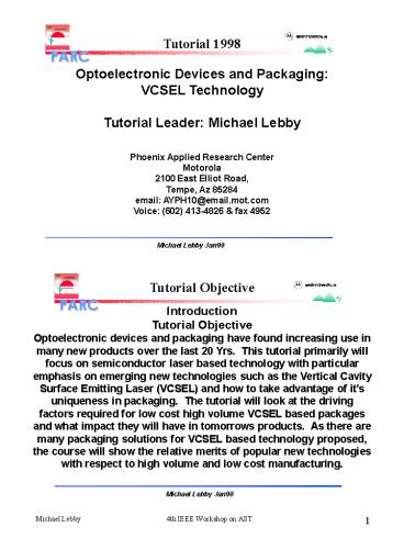
Tutorial 1998
Optoelectronic Devices and Packaging VCSEL
Technology Tutorial Leader Michael
Lebby Phoenix Applied Research
Center Motorola 2100 East Elliot Road, Tempe, Az
85284 email AYPH10_at_email.mot.com Voice (602)
413-4826 fax 4952
Tutorial Objective
Introduction Tutorial Objective Optoelectronic
devices and packaging have found increasing use
in many new products over the last 20 Yrs. This
tutorial primarily will focus on semiconductor
laser based technology with particular emphasis
on emerging new technologies such as the Vertical
Cavity Surface Emitting Laser (VCSEL) and how to
take advantage of its uniqueness in packaging.
The tutorial will look at the driving factors
required for low cost high volume VCSEL based
packages and what impact they will have in
tomorrows products. As there are many packaging
solutions for VCSEL based technology proposed,
the course will show the relative merits of
popular new technologies with respect to high
volume and low cost manufacturing.
2
Tutorial Objective
- Tutorial Objective
- Providing information that gives the attendee a
working knowledge on - Commercial Edge Emitter laser technology
- What a EE laser chip is and looks like
- How a EE laser chip is packaged
- VCSEL technology why the euphoria
- What a VCSEL chip is...
- How VCSELs are packaged...
- VCSEL Performance
- VCSEL Applications... today...tomorrow
- Technical Challenges
- Commercial and market impact
Section 1
- Section 1
- VCSEL Technology
- Device Status
- Package Status
- Section 2
- VCSEL Technical Issues
- Fabrication and Characterization
- Testing and Reliability
- Manufacturing
3
Abbreviation
V
ertical
C
avity
S
urface
E
mitting
L
aser
VCSEL (commonly pronounced 'vixel')
Other names used
Veesel (V-SEL)
VCSELD (V-seld)
VCL (Vixel)
Surface Emitter
Micro-resonator
4
Why
VCSELs
over Edge Emitters (
EEs
) ?
Component Cost Impact
Fabricated like
LEDs
-gt first laser with potential die cost to
approach
LEDs
(with high volume)
Wafer probing, no cleaving,
GaAs
saw, surface light emission
VCSELs
in high volume markets the die cost will be
similar to CD laser chips as the cost is in the
package
Die cost is sensitive to real estate (VCSEL
advantage)
Epi
wafer costs are more for VCSEL (EE advantage)
Only if the package, probe,
aligment
procedures are made LED-like will the VCSEL hope
to reach the low
cost levels expected
Packaging Cost Impact
Low volume fiber optics markets EE package cost
is 80-90 package
VCSEL should reduce this through simplified
packaging/coupling/KGD
High volume markets requires passive alignment
and KGD before package
VCSEL has potential to achieve these goals with
less volume than the EE
Trend towards LED-like packaging means plastic
alternatives are needed
System Cost Impact
VCSEL packages are smaller -gt smaller systems
VCSEL has lower power drain -gt longer battery
life on systems
VCSEL can be flip-chip packaged -gt lower cost
systems
VCSEL has circular output beam -gt less lenses in
systems
VCSEL Arrays are natural -gt provides degree of
freedom in design
EE Laser and VCSEL Output Characteristics
VCSEL
Edge emitting laser
Auto-power control (can the VCSEL avoid it?)
5
VCSEL Device Status
Structures
Planar Proton Implanted
Index Guided Ridge Waveguide
Hybrid Mirror
Intracavity contact
Lateral Oxide
Native Oxide
Wafer Fused
What is commercially available today?
Proton Implanted
Ridge Waveguide
Common device Cross-sections
Proton Isolated Planar VCSEL
Ridge Wave Guide VCSEL
6
Visible VCSEL structure
After R.
Schneider
(1995)
Partial dielectric mirror and partial
semiconductor mirror
After R.Morgan (1995)
7
(No Transcript)
8
Small signal modulation of a
lateral oxide confined VCSEL
After B.
Thibeault
, UCSB
9
Native oxide mirror VCSEL
After M.H.
MacDougal
(1995)
Wafer fused structure for long wavelength VCSEL
After J.J.Dudley (1994)
10
Commerical VCSEL Status
After Strategies Unlimited 1996
VCSEL Package Status
Packages that are being used for VCSELs
TO-can wire-bond
Plastic Leadframe Flip-chip
TAB Flip-chip
C4 Flip-chip
Efforts to address VCSEL arrays have been the
focus of many RD labs
over the last 5Yrs
A few examples are discussed
Companies participating include AMP, Gore
Photonics, MITEL, HP, Honeywell, IBM,
Lucent, Micro-optical, Picolight, SDL, Vixel,
Xerox amongst others.
Motorola's parallel link is productized (400Mbps
_at_ 10channels, 300m)
Integrated (Simplify Packaging)
Detector
Lens


