Senior Project PowerPoint PPT Presentation
1 / 1
Title: Senior Project
1
Senior Project Electrical Engineering -
2006Line-Scan Camera Timing SystemRobert
OstryeAdvisor Prof. Rudko
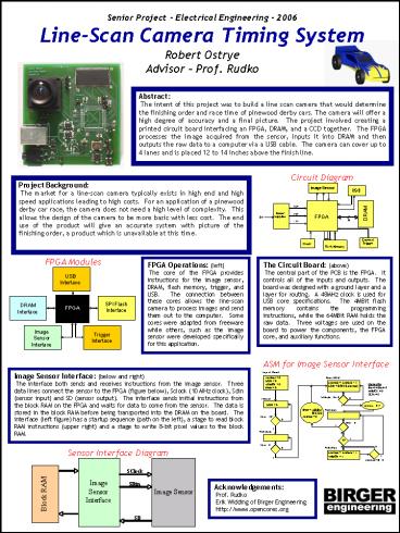
Abstract The intent of this project was to
build a line scan camera that would determine the
finishing order and race time of pinewood derby
cars. The camera will offer a high degree of
accuracy and a final picture. The project
involved creating a printed circuit board
interfacing an FPGA, DRAM, and a CCD together.
The FPGA processes the image acquired from the
sensor, inputs it into DRAM and then outputs the
raw data to a computer via a USB cable. The
camera can cover up to 4 lanes and is placed 12
to 14 inches above the finish line.
Project Background The market for a line-scan
camera typically exists in high end and high
speed applications leading to high costs. For an
application of a pinewood derby car race, the
camera does not need a high level of complexity.
This allows the design of the camera to be more
basic with less cost. The end use of the product
will give an accurate system with picture of the
finishing order, a product which is unavailable
at this time.
The Circuit Board (above) The central part of
the PCB is the FPGA. It controls all of the
inputs and outputs. The board was designed with
a ground layer and a layer for routing. A 48MHz
clock is used for USB core specifications. The
4MBit flash memory contains the programming
instructions, while the 64MBit RAM holds the raw
data. Three voltages are used on the board to
power the components, the FPGA core, and
auxiliary functions.
FPGA Operations (left) The core of the FPGA
provides instructions for the image sensor, DRAM,
flash memory, trigger, and USB. The connection
between these cores allows the line-scan camera
to process images and send them out to the
computer. Some cores were adapted from freeware
while others, such as the image sensor were
developed specifically for this application.
Image Sensor Interface (below and right) The
interface both sends and receives instructions
from the image sensor. Three data lines connect
the sensor to the FPGA (figure below), Sclock (10
MHz clock), Sdin (sensor input) and SD (sensor
output). The interface sends initial
instructions from the block RAM on the FPGA and
waits for data to come from the sensor. The data
is stored in the block RAM before being
transported into the DRAM on the board. The
interface (left figure) has a startup sequence
(path on the left), a stage to read block RAM
instructions (upper right) and a stage to write
8-bit pixel values to the block RAM.
Acknowledgements Prof. Rudko Erik Widding of
Birger Engineering http//www.opencores.org

