
Part I Background and Motivation - PowerPoint PPT Presentation
1 / 20
Title:
Part I Background and Motivation
Description:
I Background and Motivation. Chapter 4 Computer Performance ... Much like prefab closets used in building a house. Other memory components will be covered in ... – PowerPoint PPT presentation
Number of Views:50
Avg rating:3.0/5.0
Title: Part I Background and Motivation
1
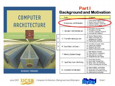
Part IBackground and Motivation
2
I Background and Motivation
- Provide motivation, paint the big picture,
introduce tools - Review components used in building digital
circuits - Present an overview of computer technology
- Understand the meaning of computer performance
- (or why a 2 GHz processor isnt 2? as fast as
a 1 GHz model)
3
2 Digital Circuits with Memory
- Second of two chapters containing a review of
digital design - Combinational (memoryless) circuits in Chapter
1 - Sequential circuits (with memory) in Chapter 2
4
2.1 Latches, Flip-Flops, and Registers
Figure 2.1 Latches, flip-flops, and
registers.
5
Latches vs Flip-Flops
Figure 2.2 Operations of D latch and
negative-edge-triggered D flip-flop.
6
Reading and Modifying FFs in the Same Cycle
Figure 2.3 Register-to-register operation
with edge-triggered flip-flops.
7
2.2 Finite-State Machines
Example 2.1
Figure 2.4 State table and state diagram for a
vending machine coin reception unit.
8
State Table for Coin Example
- Table 2.2, p. 27 (Values of Q2Q1Q0)
9
Sequential Machine Implementation
Figure 2.5 Hardware realization of Moore and
Mealy sequential machines.
10
2.3 Designing Sequential Circuits
Example 2.3
Quarter in
Final state is 1xx
Q2
Dime in
Q1
Q0
Figure 2.7 Hardware realization of a coin
reception unit (Example 2.3).
11
2.4 Useful Sequential Parts
? High-level building blocks ? Much like
prefab closets used in building a house ?
Other memory components will be covered in
Chapter 17 (SRAM details, DRAM, Flash) ? Here
we cover three useful parts shift
register, register file (SRAM basics), counter
12
Shift Register
13
Register File and FIFO
Figure 2.9 Register file with random access
and FIFO.
14
SRAM
Figure 2.10 SRAM memory is simply a large,
single-port register file.
15
Binary Counter
Figure 2.11 Synchronous binary counter with
initialization capability.
16
2.5 Programmable Sequential Parts
A programmable sequential part contain gates and
memory elements
Programmed by cutting existing connections
(fuses) or establishing new connections
(antifuses)
? Programmable array logic (PAL) ?
Field-programmable gate array (FPGA) ? Both
types contain macrocells and interconnects
17
PAL and FPGA
Figure 2.12 Examples of programmable
sequential logic.
18
2.6 Clocks and Timing of Events
Clock is a periodic signal clock rate clock
frequency The inverse of clock rate is the clock
period 1 GHz ? 1 ns Constraint Clock period ?
tprop tcomb tsetup tskew
Figure 2.13 Determining the required length of
the clock period.
19
Synchronization
Figure 2.14 Synchronizers are used to prevent
timing problems arising from untimely changes in
asynchronous signals.
20
Level-Sensitive Operation
Figure 2.15 Two-phase clocking with
nonoverlapping clock signals.
Recommended
CrystalGraphics Presentations


