
Part I Background and Motivation - PowerPoint PPT Presentation
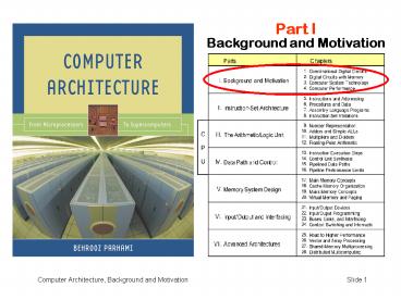
Title:
Part I Background and Motivation
Description:
Figure 1.1 Some basic elements of digital logic circuits, with operator signs ... Figure 1.4 Wired OR allows tying together of several controlled signals. ... – PowerPoint PPT presentation
Number of Views:45
Avg rating:3.0/5.0
Title: Part I Background and Motivation
1
Part IBackground and Motivation
2
I Background and Motivation
Topics in This Part
Chapter 1 Combinational Digital Circuits
Chapter 2 Digital Circuits with Memory
Chapter 3 Computer System Technology
Chapter 4 Computer Performance
3
1 Combinational Digital Circuits
Topics in This Chapter
1.1 Signals, Logic Operators, and Gates
1.2 Boolean Functions and Expressions
1.3 Designing Gate Networks
1.4 Useful Combinational Parts
1.5 Programmable Combinational Parts
1.6 Timing and Circuit Considerations
4
1.1 Signals, Logic Operators, and Gates
Figure 1.1 Some basic elements of digital
logic circuits, with operator signs used in this
book highlighted.
5
Variations in Gate Symbols
Figure 1.2 Gates with more than two inputs
and/or with inverted signals at input or output.
6
Gates as Control Elements
Figure 1.3 An AND gate and a tristate buffer
act as controlled switches or valves. An
inverting buffer is logically the same as a NOT
gate.
7
Wired OR and Bus Connections
Figure 1.4 Wired OR allows tying together of
several controlled signals.
8
Control/Data Signals and Signal Bundles
Figure 1.5 Arrays of logic gates represented
by a single gate symbol.
9
1.2 Boolean Functions and Expressions
Ways of specifying a logic function
? Truth table 2n row, dont-care in input
or output ? Logic expression w ? (x ? y ?
z), product-of-sums, sum-of-products,
equivalent expressions ? Word statement
Alarm will sound if the door is opened
while the security system is engaged, or
when the smoke detector is triggered ? Logic
circuit diagram Synthesis vs analysis
10
Manipulating Logic Expressions
Table 1.2 Laws (basic identities) of Boolean
algebra.
Name of law OR version AND version
Identity x ? 0 x x 1 x
One/Zero x ? 1 1 x 0 0
Idempotent x ? x x x x x
Inverse x ? x ? 1 x x ? 0
Commutative x ? y y ? x x y y x
Associative (x ? y) ? z x ? (y ? z) (x y) z x (y z)
Distributive x ? (y z) (x ? y) (x ? z) x (y ? z) (x y) ? (x z)
DeMorgans (x ? y)? x ? y ? (x y)? x ? ? y ?
11
Proving the Equivalence of Logic Expressions
Example 1.1
? Truth-table method Exhaustive
verification ? Arithmetic substitution
x ? y x y - xy x ? y
x y - 2xy ? Case
analysis two cases, x 0 or x 1 ? Logic
expression manipulation
Example x ? y ?? x ?y ? x y ?
x y 2xy ?? (1 x)y x(1 y) (1 x)yx(1
y)
12
1.3 Designing Gate Networks
? AND-OR, NAND-NAND, OR-AND, NOR-NOR ?
Logic optimization cost, speed, power
dissipation
(x ? y)? x ?y ?
Figure 1.6 A two-level AND-OR circuit and two
equivalent circuits.
13
BCD-to-Seven-Segment Decoder
Example 1.2
Figure 1.8 The logic circuit that generates
the enable signal for the lowermost segment
(number 3) in a seven-segment display unit.
14
1.4 Useful Combinational Parts
? High-level building blocks ? Much like
prefab parts used in building a house ?
Arithmetic components will be covered in Part
III (adders, multipliers, ALUs) ? Here
we cover three useful parts multiplexers,
decoders/demultiplexers, encoders
15
Multiplexers
Figure 1.9 Multiplexer (mux), or selector,
allows one of several inputs to be selected and
routed to output depending on the binary value of
a set of selection or address signals provided to
it.
16
Decoders/Demultiplexers
Figure 1.10 A decoder allows the selection of
one of 2a options using an a-bit address as
input. A demultiplexer (demux) is a decoder that
only selects an output if its enable signal is
asserted.
17
Encoders
Figure 1.11 A 2a-to-a encoder outputs an a-bit
binary number equal to the index of the single 1
among its 2a inputs.
18
1.5 Programmable Combinational Parts
A programmable combinational part can do the job
of many gates or gate networks
Programmed by cutting existing connections
(fuses) or establishing new connections
(antifuses)
? Programmable ROM (PROM) ? Programmable
array logic (PAL) ? Programmable logic array
(PLA)
19
PROMs
Figure 1.12 Programmable connections and their
use in a PROM.
20
PALs and PLAs
Figure 1.13 Programmable combinational logic
general structure and two classes known as PAL
and PLA devices. Not shown is PROM with fixed AND
array (a decoder) and programmable OR array.
21
1.6 Timing and Circuit Considerations
Changes in gate/circuit output, triggered by
changes in its inputs, are not instantaneous
? Gate delay d a fraction of, to a few,
nanoseconds ? Wire delay, previously
negligible, is now important (electronic
signals travel about 15 cm per ns) ? Circuit
simulation to verify function and timing
22
Glitching
Using the PAL in Fig. 1.13b to implement f x ?
y ? z
Figure 1.14 Timing diagram for a circuit that
exhibits glitching.
23
CMOS Transmission Gates
Figure 1.15 A CMOS transmission gate and its
use in building a 2-to-1 mux.
24
2 Digital Circuits with Memory
- Second of two chapters containing a review of
digital design - Combinational (memoryless) circuits in Chapter
1 - Sequential circuits (with memory) in Chapter 2
Topics in This Chapter
2.1 Latches, Flip-Flops, and Registers
2.2 Finite-State Machines
2.3 Designing Sequential Circuits
2.4 Useful Sequential Parts
2.5 Programmable Sequential Parts
2.6 Clocks and Timing of Events
25
2.1 Latches, Flip-Flops, and Registers
Figure 2.1 Latches, flip-flops, and
registers.
26
Latches vs Flip-Flops
Figure 2.2 Operations of D latch and
negative-edge-triggered D flip-flop.
27
Reading and Modifying FFs in the Same Cycle
Figure 2.3 Register-to-register operation
with edge-triggered flip-flops.
28
2.2 Finite-State Machines
Example 2.1
Figure 2.4 State table and state diagram for a
vending machine coin reception unit.
29
Sequential Machine Implementation
Figure 2.5 Hardware realization of Moore and
Mealy sequential machines.
30
2.3 Designing Sequential Circuits
Example 2.3
Quarter in
Final state is 1xx
Dime in
Figure 2.7 Hardware realization of a coin
reception unit (Example 2.3).
31
2.4 Useful Sequential Parts
? High-level building blocks ? Much like
prefab closets used in building a house ?
Other memory components will be covered in
Chapter 17 (SRAM details, DRAM, Flash) ? Here
we cover three useful parts shift
register, register file (SRAM basics), counter
32
Shift Register
33
Register File and FIFO
Figure 2.9 Register file with random access
and FIFO.
34
SRAM
Figure 2.10 SRAM memory is simply a large,
single-port register file.
35
Binary Counter
Figure 2.11 Synchronous binary counter with
initialization capability.
36
2.5 Programmable Sequential Parts
A programmable sequential part contain gates and
memory elements
Programmed by cutting existing connections
(fuses) or establishing new connections
(antifuses)
? Programmable array logic (PAL) ?
Field-programmable gate array (FPGA) ? Both
types contain macrocells and interconnects
37
PAL and FPGA
Figure 2.12 Examples of programmable
sequential logic.
38
Binary Counter
Figure 2.11 Synchronous binary counter with
initialization capability.
39
2.6 Clocks and Timing of Events
Clock is a periodic signal clock rate clock
frequency The inverse of clock rate is the clock
period 1 GHz ? 1 ns Constraint Clock period ?
tprop tcomb tsetup tskew
Figure 2.13 Determining the required length of
the clock period.
40
Synchronization
Figure 2.14 Synchronizers are used to prevent
timing problems arising from untimely changes in
asynchronous signals.
41
Level-Sensitive Operation
Figure 2.15 Two-phase clocking with
nonoverlapping clock signals.
42
3 Computer System Technology
- Interplay between architecture, hardware, and
software - Architectural innovations influence technology
- Technological advances drive changes in
architecture
Topics in This Chapter
3.1 From Components to Applications
3.2 Computer Systems and Their Parts
3.3 Generations of Progress
3.4 Processor and Memory Technologies
3.5 Peripherals, I/O, and Communications
3.6 Software Systems and Applications
43
3.1 From Components to Applications
Figure 3.1 Subfields or views in computer
system engineering.
44
What Is (Computer) Architecture?
Figure 3.2 Like a building architect, whose
place at the engineering/arts and goals/means
interfaces is seen in this diagram, a computer
architect reconciles many conflicting or
competing demands.
45
3.2 Computer Systems and Their Parts
Figure 3.3 The space of computer systems,
with what we normally mean by the word computer
highlighted.
46
Price/Performance Pyramid
Differences in scale, not in substance
Figure 3.4 Classifying computers by
computational power and price range.
47
Automotive Embedded Computers
Figure 3.5 Embedded computers are ubiquitous,
yet invisible. They are found in our automobiles,
appliances, and many other places.
48
Personal Computers and Workstations
Figure 3.6 Notebooks, a common class of
portable computers, are much smaller than
desktops but offer substantially the same
capabilities. What are the main reasons for the
size difference?
49
Digital Computer Subsystems
Figure 3.7 The (three, four, five, or) six
main units of a digital computer. Usually, the
link unit (a simple bus or a more elaborate
network) is not explicitly included in such
diagrams.
50
3.3 Generations of Progress
Table 3.2 The 5 generations of digital
computers, and their ancestors.
Generation (begun) Processor technology Memory innovations I/O devices introduced Dominant look fell
0 (1600s) (Electro-) mechanical Wheel, card Lever, dial, punched card Factory equipment
1 (1950s) Vacuum tube Magnetic drum Paper tape, magnetic tape Hall-size cabinet
2 (1960s) Transistor Magnetic core Drum, printer, text terminal Room-size mainframe
3 (1970s) SSI/MSI RAM/ROM chip Disk, keyboard, video monitor Desk-size mini
4 (1980s) LSI/VLSI SRAM/DRAM Network, CD, mouse,sound Desktop/ laptop micro
5 (1990s) ULSI/GSI/ WSI, SOC SDRAM, flash Sensor/actuator, point/click Invisible, embedded
51
IC Production and Yield
Figure 3.8 The manufacturing process for an
IC part.
52
Effect of Die Size on Yield
Figure 3.9 Visualizing the dramatic decrease
in yield with larger dies.
Die yield def (number of good dies) / (total
number of dies) Die yield Wafer yield ? 1
(Defect density ? Die area) / aa Die cost
(cost of wafer) / (total number of dies ? die
yield) (cost of wafer) ? (die area / wafer
area) / (die yield)
53
3.4 Processor and Memory Technologies
Figure 3.11 Packaging of processor, memory,
and other components.
54
Moores Law
Figure 3.10 Trends in processor performance
and DRAM memory chip capacity (Moores law).
55
3.5 Input/Output and Communications
Figure 3.12 Magnetic and optical disk memory
units.
56
Communication Technologies
Figure 3.13 Latency and bandwidth
characteristics of different classes of
communication links.
57
3.6 Software Systems and Applications
Figure 3.15 Categorization of software, with
examples in each class.
58
High- vs Low-Level Programming
Figure 3.14 Models and abstractions in
programming.
59
4 Computer Performance
- Performance is key in design decisions also cost
and power - It has been a driving force for innovation
- Isnt quite the same as speed (higher clock
rate)
Topics in This Chapter
4.1 Cost, Performance, and Cost/Performance
4.2 Defining Computer Performance
4.3 Performance Enhancement and Amdahls Law
4.4 Performance Measurement vs Modeling
4.5 Reporting Computer Performance
4.6 The Quest for Higher Performance
60
The Vanishing Computer Cost
61
Cost/Performance
Figure 4.1 Performance improvement as a
function of cost.
62
4.2 Defining Computer Performance
Figure 4.2 Pipeline analogy shows that
imbalance between processing power and I/O
capabilities leads to a performance bottleneck.
63
4.4 Performance Measurement vs. Modeling
Figure 4.5 Running times of six programs on
three machines.
64
4.5 Reporting Computer Performance
Table 4.4 Measured or estimated execution
times for three programs.
Time on machine X Time on machine Y Speedup of Y over X
Program A 20 200 0.1
Program B 1000 100 10.0
Program C 1500 150 10.0
All 3 progs 2520 450 5.6
Analogy If a car is driven to a city 100 km away
at 100 km/hr and returns at 50 km/hr, the average
speed is not (100 50) / 2 but is obtained from
the fact that it travels 200 km in 3 hours.
65
Comparing the Overall Performance
Table 4.4 Measured or estimated execution
times for three programs.
Time on machine X Time on machine Y Speedup of Y over X
Program A 20 200 0.1
Program B 1000 100 10.0
Program C 1500 150 10.0
Speedup of X over Y
10 0.1 0.1
Arithmetic mean
6.7
3.4
Geometric mean
2.15
0.46
Geometric mean does not yield a measure of
overall speedup, but provides an indicator that
at least moves in the right direction
66
4.6 The Quest for Higher Performance
State of available computing power ca. the early
2000s Gigaflops on the desktop Teraflops in
the supercomputer center Petaflops on the
drawing board Note on terminology (see Table
3.1) Prefixes for large units Kilo 103,
Mega 106, Giga 109, Tera 1012, Peta
1015 For memory K 210 1024, M 220,
G 230, T 240, P 250 Prefixes for small
units micro 10-6, nano 10-9, pico
10-12, femto 10-15
67
Supercom-puters
Figure 4.7 Exponential growth of
supercomputer performance.
Recommended
CrystalGraphics Presentations


