Compound Semiconductor Materials Industry PowerPoint PPT Presentations
All Time
Recommended
The global compound semiconductor materials market, valued at US$ 32 billion in 2022, is expected to reach US$ 65 billion by 2032, growing at a CAGR of 6% from 2022 to 2032. The Asia Pacific region is anticipated to hold the largest market share throughout the forecast period. The emergence of 5G technology is a significant driver for this market, particularly within the telecom industry, where the demand for radio frequency (RF) semiconductor devices is surging.
| PowerPoint PPT presentation | free to download
2020 Analysis and Review: Compound Semiconductor Materials Market by Application – Laser, Optical Fibers, Power Amplifiers, et al for 2020-2030
| PowerPoint PPT presentation | free to download
Sales of compound semiconductor materials to reach around US$ 2.4 Bn in 2020
| PowerPoint PPT presentation | free to download
The global Compound Semiconductor Materials market is forecast to reach USD 66.66 Billion by 2027, according to a new report by Reports and Data.
| PowerPoint PPT presentation | free to download
Sales of compound semiconductor materials to reach around US$ 2.4 Bn in 2020
| PowerPoint PPT presentation | free to download
1947 - The junction transistor was invented at Bell Lab by Bardeen, Brattain and Schockley 1958 - Integrated circuits (ICs) were invented by Kilby at TI
| PowerPoint PPT presentation | free to download
OE_50200: Compound Semiconductors. Jim Y. Chi(???) ????????. National Dong-hua University, ... What is the Moor's law for Compound Semiconductor technology? ...
| PowerPoint PPT presentation | free to view
Compound Semiconductor Market report categorizes global market by Type (III-V, II-VI, IV-IV, Sapphire), Deposition Technology (CVD, MBE, HVPE, Ammonothermal, MOVPE, LPE, ALD), Product (Power, Opto - Electronic), Application, and Geography.
| PowerPoint PPT presentation | free to download
According to the latest research report by IMARC Group, The global compound semiconductor market size reached US$ 117.7 Billion in 2023. Looking forward, IMARC Group expects the market to reach US$ 173.6 Billion by 2032, exhibiting a growth rate (CAGR) of 4.3% during 2024-2032. More Info:- https://www.imarcgroup.com/compound-semiconductor-market
| PowerPoint PPT presentation | free to download
Structured Materials Industries, Incorporated
| PowerPoint PPT presentation | free to view
According to the latest research report by IMARC Group, The global compound semiconductor market size reached US$ 112.2 Billion in 2022. Looking forward, IMARC Group expects the market to reach US$ 150.4 Billion by 2028, exhibiting a growth rate (CAGR) of 4.9% during 2023-2028. More Info:- https://www.imarcgroup.com/compound-semiconductor-market
| PowerPoint PPT presentation | free to download
The global semiconductor assembly and packaging equipment market grew from $7.99 billion in 2021 to $10.17 billion in 2022 at a compound annual growth rate (CAGR) of 27.2%.
| PowerPoint PPT presentation | free to download
A recent report published by The Business Research Company on Industrial Machinery Market provides in-depth analysis of segments and sub-segments in the global as well as regional. https://bit.ly/2xG6QWt
| PowerPoint PPT presentation | free to download
The major players covered in the Industrial Machinery Market are ASML Holdings, Tokyo Electron, LAM Research, Tetra Pak, Applied Materials.. @ @ http://bit.ly/3sNBzaH
| PowerPoint PPT presentation | free to download
The Business Research Company published an exclusive report, titled, “Industrial Machinery Market - Opportunities and Strategies, 2021-2030, which offers a detailed analysis of prime factors that impact the market growth. https://bit.ly/33DxkUE
| PowerPoint PPT presentation | free to download
TBRC global semiconductor assembly and packaging equipment market report includes plating equipment, inspection and dicing equipment, wire bonding equipment https://bit.ly/37yaLpW
| PowerPoint PPT presentation | free to download
TBRC global semiconductor assembly and packaging equipment market report includes plating equipment, inspection and dicing equipment, wire bonding equipment https://bit.ly/37yaLpW
| PowerPoint PPT presentation | free to download
Hong Kong is ranked 11th and China 50th. Engineers in Society Lecture Series -0.01 ... and service IT is the fastest growing part in China's IT industry ...
| PowerPoint PPT presentation | free to view
... Advancement on novel gain materials based on III-V-N semiconductors and GaInN Train early career ... and conferences led by scientists in the ...
| PowerPoint PPT presentation | free to download
Wire insulation & jacketing compounds are plastic compounds which find applications in the manufacture of wire & cable insulation products used for protecting & insulating and jacketing wires & cables. A diverse set of properties is imparted to wire insulation & jacketing compounds, which primarily depend on applications and item operating conditions.
| PowerPoint PPT presentation | free to download
Lipids are termed as a large organic compounds that fall under the classes of fatty acid derivatives or closely related compounds. Lipids are generally insoluble in water but exhibit high levels of solubility in organic solvents & alcohols.
| PowerPoint PPT presentation | free to download
The companies and manufacturers get an understanding into the upstream raw material analysis and downstream demand survey and tracks the impact of market dynamics on industry chain structure.
Compound semiconductors are the materials formed with the combination of two or more elements. Compound semiconductors are not available in nature and have to be synthesized using various deposition technologies. The properties possessed by compound semiconductors are unique and advantageous over other elemental materials
Conductive plastics conduct electricity and have properties of semiconductors or metallic conductors. This kind of plastics are generally conducting polymers which are formulated by organic polymers to conduct electricity. These compounds are reliable and provide static discharge and protection from Electro-Static Discharge (ESD). These organic polymers are inexpensive and lighter in weight than any other conventional materials such as metals and ceramics hence are widely used in several industrial applications
| PowerPoint PPT presentation | free to download
Semiconductors are materials that conduct electricity better than insulators like ceramics, but not as well as conductors like metals. They can be compounds like gallium arsenide or pure elements like germanium or silicon. The function of semiconductor is to control and manage the flow of electric current in electronic equipment and devices. From smartphones to home appliances, cars, transportation, and medical devices, semiconductors power almost all the technology that we rely on today
| PowerPoint PPT presentation | free to download
Semiconductor Market
| PowerPoint PPT presentation | free to download
The Global MO (Metal Organic) Source Industry Market Outlook research report delivers an in-depth assessment of the current Materials and Chemicals industry status and future outlook. With thealysis, you get an idea of how the industry is predictable to change.
| PowerPoint PPT presentation | free to download
The Business Research Company offers opto semiconductors market research report 2023 with industry size, share, segments and market growth
| PowerPoint PPT presentation | free to download
Epitaxial wafers are a key component in the semiconductor industry. They are used to produce high-quality, single-crystal layers of semiconductor materials on a substrate, which are then used in the manufacturing of various electronic devices. These wafers are essential for the production of advanced semiconductors, such as integrated circuits, power devices, and sensors. The demand for epitaxial wafers is driven by the growing need for advanced and efficient electronic devices across various industries.
| PowerPoint PPT presentation | free to download
The Business Research Company offers gallium nitride semiconductor devices market research report 2023 with industry size, share, segments and market growth
| PowerPoint PPT presentation | free to download
Semiconductor Devices and Physics (Ch. 1) Why semiconductor? Foundation of the electronic industry Including applied physics, electrical engineering, electronics ...
| PowerPoint PPT presentation | free to view
Global Thin Film Semiconductor Deposition Market is estimated to reach $36 billion by 2025; growing at a CAGR of 14.1% from 2017 to 2025.Thin film semiconductors, the foils made from artificial semiconductor materials have the thickness from nanometers to few hundred millimeters.
| PowerPoint PPT presentation | free to download
Ion beam is a type of charged particle beam containing of ions. Ion beam technology is an advanced method that is being mainly used for semiconductor industry, and also increasingly tapped in the organic field for the use of ablation & deposition of materials and site-specific analysis
| PowerPoint PPT presentation | free to download
Antioxidants for polymer materials refer to chemical substances that can inhibit or delay the oxidative degradation of polymer materials by oxygen or ozone in the atmosphere, thereby preventing material aging and prolonging service life. Antioxidants can be divided into main antioxidants and auxiliary antioxidants. Among them, main antioxidants can eliminate free radicals in the resin system, mainly aromatic amines and hindered phenolic compounds and their derivatives; auxiliary antioxidants can eliminate free radicals in the resin system. The hydroperoxides in the resin system are decomposed in time, mainly the organic compounds containing phosphorus and sulfur.For more information, please contact the following e-mail address: Email: global@qyresearch . com Website: https://www . qyresearch . com
| PowerPoint PPT presentation | free to download
Water treatment is used to optimize most water-based industrial processes, such as: heating, cooling, processing, cleaning, and rinsing, so that operating costs and risks are reduced. Poor water treatment lets water interact with the surfaces of pipes and vessels which contain it. Steam boilers can scale up or corrode, and these deposits will mean more fuel is needed to heat the same amount of water. Cooling towers can also scale up and corrode, but left untreated, the warm, dirty water they can contain will encourage bacteria to grow, and Legionnaires’ Disease can be the fatal consequence. Also, water treatment is used to improve the quality of water contacting the manufactured product e.g. semiconductors, and/or can be part of the product e.g. beverages, pharmaceuticals, etc. In these instances, poor water treatment can cause defective products.
| PowerPoint PPT presentation | free to download
... Main application of semiconductors are transistors ... industries (12%), automobiles (5%), and ... and Environmental Technology (Uo2, Ni ...
| PowerPoint PPT presentation | free to view
India Fluorinated Organic Compounds Market
| PowerPoint PPT presentation | free to download
UNIT 1 MATERIALS Vocabulary Names of materials Characteristics of materials Adjectives and dimensions Word formation: SUFFIXES to form ADJECTIVES
| PowerPoint PPT presentation | free to download
UNIT 1 MATERIALS Vocabulary Names of materials Characteristics of materials Adjectives and dimensions Word formation: SUFFIXES to form ADJECTIVES
| PowerPoint PPT presentation | free to view
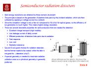
Best energy resolutions are obtained by these sensors at present The principle is based on the generation of electron-hole pairs by the incident radiation, which are ...
| PowerPoint PPT presentation | free to download
Global 3D Semiconductor Packaging Market is estimated to reach $12 Billion by 2024; growing at a CAGR of 15.2% from 2016 to 2024.
| PowerPoint PPT presentation | free to download
Both, copper grade and nickel grade anti-seize compounds find immense utilization across every end-use industry, the latter particularly being used in the petrochemical and oil & gas sectors, owing to their inert nature. Shareholders would generate around 25% of total return from copper grade anti-seize compounds, compared to 12% from the nickel grade version. However, the usage of both these grades is likely to falter by the end of forecast period amidst ecological burden.
| PowerPoint PPT presentation | free to download
Bharat Book Bureau provides the report, on “The Global Market Report on Electronic chemicals and Materials ” The Report Provide basic View on Electronic chemicals and materials are solid, liquid and gaseous substances used in the fabrication of semiconductors and printed circuit boards (PCBs).
| PowerPoint PPT presentation | free to download
SMC market is expected to prosper at a healthy CAGR of 5.0% during 2021-2026 to reach the figure of US$ 3.6 Billion in 2026.
| PowerPoint PPT presentation | free to download
Many free electrons not tied up in chemical bonds. Insulators. All electrons (in intrinsic material) tied up in chemical bonds ...
| PowerPoint PPT presentation | free to download
The Perovskite Solar Cells market report offers an insightful analysis of industry outlooks, market dynamics, opportunities and revenue forecast. Get a Copy of the Report @ https://www.adroitmarketresearch.com/industry-reports/perovskite-solar-cells-market
| PowerPoint PPT presentation | free to download
Global 3d semiconductor packaging market size is expected to reach $29.17 Bn by 2028 at a rate of 16.2%, segmented as by type, 3d through silicon via, 3d package on package, 3d fan out based, 3d wire bonded
| PowerPoint PPT presentation | free to download
MAE 438/538 Smart Materials Professor Deborah Chung ddlchung@buffalo.edu Furnas Hall, Room 608 Tel. (716) 645-2593 X2243 Fax. (716) 645-3875 Grading scheme for MAE ...
| PowerPoint PPT presentation | free to download
According to the latest research report by IMARC Group, The global semiconductor dry strip systems market size reached US$ 377.8 Million in 2023. Looking forward, IMARC Group expects the market to reach US$ 563.2 Million by 2032, exhibiting a growth rate (CAGR) of 4.4% during 2024-2032. More Info:- https://www.imarcgroup.com/semiconductor-dry-strip-systems-market
| PowerPoint PPT presentation | free to download
The semiconductor packaging market is expected to leverage high potential for consumer electronics and automotive verticals. The current business scenario is witnessing an increasing demand for consumer electronics devices, particularly in developing countries such as China, Japan, South Korea, India, and others. Companies in this industry are adopting various innovative techniques, such as merger & acquisition activities, to strengthen their business position in the competitive matrix.
| PowerPoint PPT presentation | free to download
High performance fluoropolymers are polymers which contain fluorocarbon compounds and have unique characteristics such as high mechanical strength, low coefficient of friction, excellent electrical insulation, resistance against chemical environment and elevated temperature. High performance fluoropolymers provides better efficiency as compared to conventional materials.
| PowerPoint PPT presentation | free to download
The report titled Sucrose Esters Market is an in-depth and a professional document that provides a comprehensive overview of the Industry.
| PowerPoint PPT presentation | free to download
Sputter Coatings Market,segmented into the target material, substrate, and application industry. On the basis of the target material, the market is segmented into the pure material, alloys, compounds, and others. On the basis of the substrate, the global sputter coatings market is segmented into ceramic, metals & dielectric, glass, plastic, semiconductors, and others. On the basis of the application, the market is bifurcated into automotive & transportation, architecture, electrical & electronics, defense, energy, optical coatings, tribological coatings, and others. Free Request Sample @ https://www.marketresearchfuture.com/sample_request/5655
| PowerPoint PPT presentation | free to download
... (continued) Electrical power transmission Eddy current inspection (use of a magnetically induced electrical current to indicate flaws in a material) ...
| PowerPoint PPT presentation | free to download
Title: No Slide Title Author: Leslie Zaitz Last modified by: Dieter Bergman Created Date: 9/14/1999 7:21:44 PM Document presentation format: On-screen Show
| PowerPoint PPT presentation | free to view
Global organic electronics market size is expected at $124.01 Bn by 2028 at a growth rate of 19.0% and share analysis by The Business Research Company.
| PowerPoint PPT presentation | free to download


