Silicon Cmp PowerPoint PPT Presentations
All Time
Recommended
RF Pads : schematics and simulation models. - With or without ESD ... Opto-electronic circuits (Sapphire is Transparent) ISO 9002 CERTIFIED. http://cmp.imag.fr ...
| PowerPoint PPT presentation | free to view
industrial quality process lines (University process lines cannot offer a stable ... Dual-damascene copper for interconnect. 6 to 9 metal layers for interconnect ...
| PowerPoint PPT presentation | free to view
Modeling of CMP David Dornfeld CMP researchers: Jihong Choi, Sunghoon Lee, Dr. Hyoungjae Kim, Dr. Dan Echizenya Department of Mechanical Engineering
| PowerPoint PPT presentation | free to download
These are some of the sample reports that we provide for business's across the globe, to which is helpful to gain some insights of opportunities and other changes in market for various business sectors accordingly.
| PowerPoint PPT presentation | free to download
Area Fill Synthesis Algorithms for Enhanced VLSI Manufacturability Department of Computer Science University of Virginia Y. Chen, A. B. Kahng, G. Robins, A. Zelikovsky
| PowerPoint PPT presentation | free to download
Microthreaded models for CMPs IFIP 10.3 Seminar 6/12/2005 By Chris Jesshope University of Amsterdam Motivation Problems and opportunities in designing chip multi ...
| PowerPoint PPT presentation | free to download
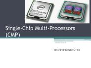
Single-Chip Multi-Processors (CMP) ELEC6200-001, Fall 08 PRADEEP DANDAMUDI Microprocessor Methods To Increase Performance: The number of transistors available has a ...
| PowerPoint PPT presentation | free to download
Post-CMP wafer topography depends on metal density, individual ... Standalone, ECO, and ripup-refill use models. Supports thickness bias models (CMP predictors) ...
| PowerPoint PPT presentation | free to view
The research report has incorporated the analysis of different factors that augment the market?s growth. It constitutes trends, restraints, and drivers that transform the market in either a positive or negative manner. This section also provides the scope of different segments and applications that can potentially influence the market in the future. The detailed information is based on current trends and historic milestones.
| PowerPoint PPT presentation | free to download
To separate a thin device layer from the bulk of the wafer. by inserting an electrically insulating layer. Insulator, 0.1 10 um ... Source: Ibis, www.ibis.com ...
| PowerPoint PPT presentation | free to view
Title: Fill for Shallow Trench Isolation CMP Author: Puneet Sharma Last modified by: Puneet Sharma Created Date: 11/4/2003 12:28:36 AM Document presentation format
| PowerPoint PPT presentation | free to download
Single-Chip Multi-Processors (CMP) ELEC6200-001, Fall 08 PRADEEP DANDAMUDI Microprocessor Methods To Increase Performance: The number of transistors available has a ...
| PowerPoint PPT presentation | free to download
3D CMP and 3D IC Physical Design Flow Jason Cong and Guojie Luo University of California, Los Angeles {cong, gluo}@cs.ucla.edu Outline Design Driver 3D Chip ...
| PowerPoint PPT presentation | free to download
... VLSI CAD Laboratory UC San Diego Computer Engineering VLSI CAD Laboratory ... Chemical mechanical planarization (CMP) critical process step in STI to remove ...
| PowerPoint PPT presentation | free to download
Caterpillar Cat 267 Multi Terrain Loader (Prefix CMP) Service Repair Manual Instant Download (CMP00001)
Investigation of the Effects of the Wafer-Pad Contact Mode on CMP Performance SFR Workshop November 8, 1999 Yongsik Moon, Andrew Chang, Jianfeng Luo,
| PowerPoint PPT presentation | free to download
Caterpillar Cat 267 Multi Terrain Loader (Prefix CMP) Service Repair Manual Instant Download (CMP00001)
Applications may contain much instruction level parallelism ... Graph needs 3 colors (chromatic nr =3) = program needs 3 registers. H.C. TD 5102. 30 ...
| PowerPoint PPT presentation | free to view
Caterpillar Cat 267 Multi Terrain Loader (Prefix CMP) Service Repair Manual Instant Download (CMP00001)
Example: avoiding one-cycle load interlock. Code: a = b c d = e - f. Unscheduled code: ... Sub R4,R1,R2 interlock. Sw d,R4. Scheduled code: Lw R1,b. Lw R2,c ...
| PowerPoint PPT presentation | free to download
Johann M. Heuser, GSI Darmstadt, Germany. for the CBM Collaboration ... Detailed simulations being prepared. Study impact on physics. ...
| PowerPoint PPT presentation | free to download
System Drivers Chapter. Defines the IC products that drive manufacturing and design technologies ... previous generation one, but provides only 50% more ...
| PowerPoint PPT presentation | free to view
CMP Slurry Market
| PowerPoint PPT presentation | free to download
Silicon Diffractive Optics for Infrared Spectroscopy Dan Jaffe
| PowerPoint PPT presentation | free to download
Computer Science Jeopardy Computer Science Jeopardy Computer Science Jeopardy $100 Question from CMPS $100 Answer from CMPS $200 Question from CMPS $200 Answer from ...
| PowerPoint PPT presentation | free to view
Fabrication of advanced metallization (deposition and CMP) ... Damascene & CMP. Project: Chemical Mechanical Polishing of Copper. IDR - HC. CVD barriers for Cu ...
| PowerPoint PPT presentation | free to view
... MS2001 Dump-rinse Spin Dry Inspection Post ICP Deep Silicon Etch Polymer Removal Clean CMOS/Non ... Technology Gene Chip Compound Semiconductor ...
| PowerPoint PPT presentation | free to download
FLCC Seminar Title: Effects of CMP Slurry Chemistry on Agglomeration of Alumina Particles and Copper Surface Hardness Faculty: Jan B. Talbot Student: Robin Ihnfeldt
| PowerPoint PPT presentation | free to download
IC Fabrication and ... from a dopant-containing ambient or doped solid source Formation of Insulating Films The favored insulator is pure silicon ...
| PowerPoint PPT presentation | free to download
Chapter 2. Introduction of IC Fabrication. 9/7/09. 2. Outlines ... IC Fabrication Process Module. Photolithography. Thin film growth, dep. and/or CMP. Etching ...
| PowerPoint PPT presentation | free to view
Member of the Scientific Board and Supervisory Board of FhG-ISE and ISFH, ... Inverters (DK), PV Silicon (DE), Q-Cells (DE), Samsung Deutschland (DE), Sanyo ...
| PowerPoint PPT presentation | free to view
Laser Re-Crystallization uses a laser to scan polycrystalline silicon on the ... it and allowing it to re-crystallize forming a single-crystal material matched ...
| PowerPoint PPT presentation | free to view
Designs the ARM range of RISC processor cores ... to semiconductor partners who fabricate and sell to their customers. ARM does not fabricate silicon itself ...
| PowerPoint PPT presentation | free to view
Trevor Burton. Multiprocessors for DSP. SYSC5603 Digital Signal Processing ... M. Chen and K. Olukotun, 'The Stanford Hydra CMP', IEEE Micro, vol. 20, no. 2, ...
| PowerPoint PPT presentation | free to download
The single damascene stacks consisted 50nm silicon carbide (SiC:H, k=4.5) etch ... Median leakage currents at 1MVcm-1 from single damascene inter-digitated comb ...
| PowerPoint PPT presentation | free to view
... completely new kinds of stuff: that's what materials science is all ... One of these materials - silicon - is making it possible for today's technology. ...
| PowerPoint PPT presentation | free to download
This tutorial will cover 'the latest word' in physical chip implementation ... minimum area rules for stacked vias. CMP (chemical mechanical polishing) area fill rules ...
| PowerPoint PPT presentation | free to view
... photoresist strip, silicon nitride deposition from front and backside (4) e-beam deposition of Ta-Ti-Cu seed on backside (5) Cu electro-plating to close bottom of ...
| PowerPoint PPT presentation | free to download
The LNS system is a perfect fit for characterizing size distribution of particles in post CMP cleaning effluent with its high sizing resolution, absolute concentration measurement, fast-response, and online, real-time monitoring capability.
| PowerPoint PPT presentation | free to download
Chemical Mechanical Planarization (CMP) Slurry market has shown significant growth in the historical years and its market stood at 53.98 thousand tonnes as of 2021 and is anticipated to grow with a healthy CAGR of 5.03% in forecast years until 2035. Chemical Mechanical Planarization (CMP) Slurry Market Analysis: Type, End Uses, Distribution Channel, Regional Demand, 2015-2035.
The Scanning Threshold Particle Counter from Kanomax FMT is the world’s only online UPW particle measurement tool for 10-20nm particles. Unlike optical particle counters, the particles are counted regardless of their composition and refractive index. Request a quote today.
| PowerPoint PPT presentation | free to download
Material preparation is the beginning of the process in making an IC chip. ... antimony and melted at 1400 in a quartz crucible surrounded by an inert gas ...
| PowerPoint PPT presentation | free to view
B2H6, burnt chocolate, sickly sweet odor. Poisonous, flammable, and explosive. N-type dopants ... NH3, pungent, irritating odor, corrosive. Dopants for ...
| PowerPoint PPT presentation | free to view
According to the latest research report by IMARC Group, The Vietnam semiconductor materials market size reached US$ 4.4 Billion in 2023. Looking forward, IMARC Group expects the market to reach US$ 11.5 Billion by 2032, exhibiting a growth rate (CAGR) of 11% during 2024-2032. More Info:- https://www.imarcgroup.com/vietnam-semiconductor-materials-market
| PowerPoint PPT presentation | free to download
Gate Oxide Integrity And Microloading Characterization of 300mm ... The main difference was a large and increasing hysteresis behavior on successive wafer runs. ...
| PowerPoint PPT presentation | free to view
... LOCOS as preferred isolation technology. STI vs. LOCOS Isolation Schemes ... Wafer Pressure (# not correct, computer can't control the down force automatically) ...
| PowerPoint PPT presentation | free to download
This project is driven by an increasing demand for vanishingly ... Edge chips. Sub-surface damage. Scratches. Curled/Wavy die. Particulate embedded in die face ...
| PowerPoint PPT presentation | free to download
R&R Industries is a leader in the Commercial Roofing and Sheet Metal Industry since 1948 in Orlando, Florida, USA. We have provided excellent service for more than 70 years and will continue to do so for many more years to come.
| PowerPoint PPT presentation | free to download
Title: Hyperthreading Author: Neilin Chakrabarty Last modified by: Zoran Jovanovic Created Date: 4/3/2004 3:49:55 AM Document presentation format
| PowerPoint PPT presentation | free to download
MonolithIC 3D ICs RCAT approach MonolithIC 3D Inc. , Patents Pending * MonolithIC 3D Inc. , Patents Pending 3D ICs at a glance A 3D Integrated Circuit is a chip that ...
| PowerPoint PPT presentation | free to download
As per Delvens market research analysis, the global electronic chemicals and materials market has reached USD 59.7 billion by 2021 and growing at a CAGR of 6.5% during the forecasting period, 2022-2028.
| PowerPoint PPT presentation | free to download
According to the latest research report by IMARC Group, The India semiconductor materials market size reached US$ 4.5 Billion in 2022. Looking forward, IMARC Group expects the market to reach US$ 6.5 Billion by 2028, exhibiting a growth rate (CAGR) of 6.3% during 2023-2028. More Info:- https://www.imarcgroup.com/india-semiconductor-materials-market
| PowerPoint PPT presentation | free to download
Semiconductors are the physical representation of a logic (software) function Fabricating semiconductors is converting software into a physical circuit
| PowerPoint PPT presentation | free to download
Advanced Semiconductor Substrates by Heterogeneous Integration Nathan Cheung Dept of EECS, UC-Berkeley cheung@eecs.berkeley.edu SOI SSOI GeOI
| PowerPoint PPT presentation | free to download
193nm lithography will continue as the main chip manufacturing workhorse for at ... Use our design-oriented lithography simulation to generate litho-hotspots ...
| PowerPoint PPT presentation | free to download


