Rambus PowerPoint PPT Presentations
All Time
Recommended
Title: Memory Issues in Graphics Hardware Author: Bob Reese Last modified by: Robert B. Reese Created Date: 2/18/1998 10:23:58 PM Document presentation format
| PowerPoint PPT presentation | free to download
MBA's Legal Issues in Mortgage Technology Conference November 30 December 2, 2005 ... Royalty Free Licencing. RAND Approach. Key case: Wang, Dell, and Rambus. Q&A ...
| PowerPoint PPT presentation | free to view
2-1/2D Organization of a 64-Word by One-Bit RAM. 7-9. Chapter 7 - Memory ... Rambus technology on the Nintendo 64 motherboard (top left and bottom right) ...
| PowerPoint PPT presentation | free to view
DRAM consists of a Transistor and a Capacitor are ... SDRAM. DDR SDRAM. DDR2 SDRAM. RDRAM. VRAM. SGRAM. RAMBUS. Memory. Memory Manufacturers: www.crucial.com ...
| PowerPoint PPT presentation | free to view
Memory is separate from the CPU. All data is in binary ... (Newer still): SDRAM, RamBus. Pages 158 to 160. ITEC 1011. Introduction to Information Technologies ...
| PowerPoint PPT presentation | free to view
What Are Various IP Regimes and What Are Key Developments in such Regimes ... Motor City Bagel (1999) Hughes (1987) Monsanto (1980s) Rambus (2004) DuPont (1970s) ...
| PowerPoint PPT presentation | free to view
poor performance of one single node might be sufficient ... Intel 860 Chip Set. Intel 1.5 GHz Xeon CPU. Up to 2 GB Rambus Memory. Five 64 bit 66Mhz PCI slots ' ...
| PowerPoint PPT presentation | free to view
Mark Twain's Connecticut Yank went to Warwick Castle, England. ... What was the first thing he did in power? ... Agencies overturning courts (FTC Rambus, ITC Tessera) ...
| PowerPoint PPT presentation | free to view
Samsung vs. Apple ...
| PowerPoint PPT presentation | free to view
Alpha 21364 Goal: very fast multiprocessor systems, highly scalable Main trick is high-bandwidth, low-latency data access. How to do it, how to do it?
| PowerPoint PPT presentation | free to download
Global Memristor Market is estimated to reach $465 million by 2024; growing at a CAGR of 80.1% from 2016 to 2024. Memristor is a memory device, which also work as a resistor in the circuit. The important feature of memristor is that, it has the ability to retain its resistance value during power cut. Various attractive features such as short read & write timing, compact size, and high retention is raising the popularity of memristors among wide application areas such as IT & telecommunication, defense, electronics, industrial, automotive, and healthcare.
| PowerPoint PPT presentation | free to download
Title: I. The Sociological Perspective. Author: mjansson Last modified by: wegnerp Created Date: 1/4/2000 4:29:28 AM Document presentation format
| PowerPoint PPT presentation | free to download
(memory) ram & rom
| PowerPoint PPT presentation | free to view
Dynamic RAM (DRAM) Used in main memory. Bits stored as charge ... Synchronous DRAM (SDRAM) Access is synchronized with an ... (CPU waits in conventional DRAM) ...
| PowerPoint PPT presentation | free to download
Main trick is high-bandwidth, low-latency data access. How to do it, how to do it? ... Each CPU directly controls its main memory chips (no intervening chipset) ...
| PowerPoint PPT presentation | free to view
William Stallings Computer Organization and Architecture 6th Edition Chapter 5 Internal Memory (revised 9/24/02) * * Semiconductor Memory Types Semiconductor Memory ...
| PowerPoint PPT presentation | free to download
Bits stored as on/off switches. No charges to leak. No ... A bit per chip system has 16 lots of 1Mbit chip with bit 1 of each word in chip 1 and so on ...
| PowerPoint PPT presentation | free to download
William Stallings Computer Organization and Architecture 7th Edition Chapter 5 Internal Memory ...
| PowerPoint PPT presentation | free to view
Intellectual Property and the Mortgage Industry: A Primer Gabe Minton, VP Industry Technology, MBA
| PowerPoint PPT presentation | free to view
Sync DRAM next Tuesday. Project 1 Discussion Switch Debouncing ... Synchronous DRAM (SDRAM) Access is ... RAM finds data (CPU waits in conventional DRAM) ...
| PowerPoint PPT presentation | free to download
Internal Memory (revised 9/24/02) ... non-destructive No permanent damage to memory Detected using Hamming error correcting code Interleaved Memory Collection of DRAM ...
| PowerPoint PPT presentation | free to download
Map MCC codes to expense ... MCC code level e.g. Airline transactions could have a higher ... to win a Nintendo Wii !!! Other Ubex Presentations ...
| PowerPoint PPT presentation | free to download
William Stallings Computer Organization and Architecture 7th Edition Chapter 5 Internal Memory
| PowerPoint PPT presentation | free to view
... or rules governing storage and destruction of documents or ESI. ... had a documented retention policy...why couldn't they destroy docs under that program? ...
| PowerPoint PPT presentation | free to view
The Alpha 21264 Data Stream Matt Ziegler
| PowerPoint PPT presentation | free to download
Title: PowerPoint Last modified by: SYSOP Created Date: 1/1/1601 12:00:00 AM Document presentation format: Other titles: Times New Roman Arial ...
| PowerPoint PPT presentation | free to view
Speech Recognition. Financial Modeling (stock options, derivatives) ... Memory in all chips is visible. Access via the inter-chip network ...
| PowerPoint PPT presentation | free to download
Storage capacity is measured in megabytes (MB) Random Access Memory (RAM) ... Speed = thousands of megabytes per second (MB/s) Types of Memory ...
| PowerPoint PPT presentation | free to view
Title: Milly Watt Project Author: Carla Ellis Last modified by: Carla Ellis Created Date: 12/3/1999 7:40:16 AM Document presentation format: On-screen Show
| PowerPoint PPT presentation | free to download
Title: Slide 1 Author: ajardine Last modified by: j.nicholson-biss Created Date: 11/16/2006 5:03:56 PM Document presentation format: On-screen Show
| PowerPoint PPT presentation | free to download
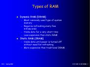
Types of RAM Dynamic RAM (DRAM) Most commonly used type of system memory Requires refreshing every few milliseconds Holds data for a very short time
| PowerPoint PPT presentation | free to download
Organizacao de Computadores: Memoria - CIn - Centro de ... ... Mem ria
| PowerPoint PPT presentation | free to download
Need to do: chip layout and fabrication development of the compiler. Funds needed for: ... Fabricate chips. Build a workstation with an intelligent memory system ...
| PowerPoint PPT presentation | free to download
William Stallings Computer Organization and Architecture 6th Edition Chapter 5 Internal Memory Semiconductor Memory Types Semiconductor Memory RAM Misnamed as all ...
| PowerPoint PPT presentation | free to view
... complete two instructions per clock cycle, effectively doubling the speed ... Blue Screen of Death. are most likely related to: badly fragmented hard drives, ...
| PowerPoint PPT presentation | free to view
The Cell Processor: Technological Breakthrough or Yet Another Over-hyped Chip?
| PowerPoint PPT presentation | free to download
William Stallings Computer Organization and Architecture 8th Edition Chapter 5 Internal Memory Semiconductor Memory Types Semiconductor Memory RAM Misnamed as all ...
| PowerPoint PPT presentation | free to download
Double clocked cache. 6. Pipelined Cache Access. Alpha 21264 Data cache design ... Cache clock frequency doubles processor frequency; wave pipelined to achieve the ...
| PowerPoint PPT presentation | free to download
RAS cycle fetched rows of data from cell array blocks (long access time, around 100ns) ... During RAS operation, address lines select the bank and row ...
| PowerPoint PPT presentation | free to view
32/64-bit Dirac Kernel, LQCD (Martin L scher, (DESY) CERN, 2000) ... 32-bit Architectures (e.g. IA32) have a much better price performance ratio than ...
| PowerPoint PPT presentation | free to download
Memory Part II Memory Technologies 2 ways to store a state electrically Determine if charge is present Determine if current will flow Can also be done magnetically ...
| PowerPoint PPT presentation | free to download
Multiple CAS accesses: several names (page mode) Extended Data Out (EDO): 30% faster in page mode New DRAMs to address gap; what will they cost, will they survive?
| PowerPoint PPT presentation | free to download
A+ Certification Guide Chapter 5 Random Access Memory Chapter 5 Objectives RAM Basics: Describe what RAM does, how it works, and how it relates to the system.
| PowerPoint PPT presentation | free to download
1100 signal pins in flip chip packaging. Better answers. EV8 Architecture Overview. Enhanced out-of-order execution. 8-wide superscalar. Large on-chip L2 cache ...
| PowerPoint PPT presentation | free to download
Introducing the TDS6000C Best Real-time Oscilloscope
| PowerPoint PPT presentation | free to download
Exploiting Locality in DRAM
- Exploiting Locality in DRAM Xiaodong Zhang College of William and Mary
Exploiting Locality in DRAM Xiaodong Zhang College of William and Mary
| PowerPoint PPT presentation | free to download
Power Considerations in Mobile Devices
| PowerPoint PPT presentation | free to download
Effective Use of Intellectual Property Data for Competitive Business Intelligence ... Lexis Nexis. New Web Vendors. Micropatent. Delphion. NERAC ...
| PowerPoint PPT presentation | free to download
HiDISC: A Decoupled Architecture for Applications in Data Intensive ... (FLIR SAR VIDEO ATR /SLD Scientific ) Processor. Decoupling Compiler. HiDISC Processor ...
| PowerPoint PPT presentation | free to download
Miles Murdocca and Vincent Heuring Chapter 7 Memory Chapter Contents 7.1 The Memory Hierarchy 7.2 Random-Access Memory 7.3 Memory Chip Organization 7.4 Case Study ...
| PowerPoint PPT presentation | free to view
A high-density DRAM package alternative consisting of several components ... Acronym for Static Random Access Memory which is an integrated circuit similar ...
| PowerPoint PPT presentation | free to view
RAS. CAS. ADD. Data. OE. RADD. CADD. PreAmps. Decoder. FPM/EDO. Based on standard DRAM core. Fast random access on data within a row (single RAS, multiple CAS) ...
| PowerPoint PPT presentation | free to view
16 GB/s total read/write bandwidth. 16 Victim buffers for L1 - L2 ... 30ns CAS latency pin to pin. 6 GB/sec read or write bandwidth. 100s of open pages ...
| PowerPoint PPT presentation | free to download
Controls physical aspect ratio. In DRAM, allows reuse of chip address pins. Spring 2002 ... On-chip circuitry (FSM) to control erasure and programming (writing) ...
| PowerPoint PPT presentation | free to download
Continuing the Performance Lead Beyond Y2K. Shubu Mukherjee, Ph.D. Principal Hardware Engineer ... Performance Lead Beyond Y2K. Better answers. My Current ...
| PowerPoint PPT presentation | free to download
William Stallings Computer Organization and Architecture 7th Edition Chapter 5 Internal Memory Semiconductor Memory Types Semiconductor Memory RAM Misnamed as all ...
| PowerPoint PPT presentation | free to view


