LLRF System Clock PowerPoint PPT Presentation
Title: LLRF System Clock
1
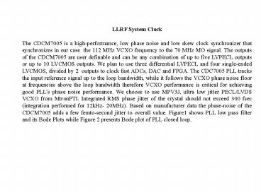
LLRF System Clock The CDCM7005 is a
high-performance, low phase noise and low skew
clock synchronizer that synchronizes in our case
the 112 MHz VCXO frequency to the 70 MHz MO
signal. The outputs of the CDCM7005 are user
definable and can be any combination of up to
five LVPECL outputs or up to 10 LVCMOS outputs.
We plan to use three differential LVPECL and four
single-ended LVCMOS, divided by 2 outputs to
clock fast ADCs, DAC and FPGA. The CDC7005 PLL
tracks the input reference signal up to the loop
bandwidth, while it follows the VCXO phase noise
floor at frequencies above the loop bandwidth
therefore VCXO performance is critical for
achieving good PLLs phase noise performance. We
choose to use MPV3J, ultra low jitter PECL/LVDS
VCXO from MtronPTI. Integrated RMS phase jitter
of the crystal should not exceed 300 fsec
(integration performed for 12kHz- 20MHz). Based
on manufacturer data the phase-noise of the
CDCM7005 adds a few femto-second jitter to
overall value. Figure1 shows PLL low pass filter
and its Bode Plots while Figure 2 presents Bode
plot of PLL closed loop.
2
Fig.1
3
Figure 2 The Bode Plot for PLL Closed Loop
4
We decided to use strip line for clock
distribution because of two reasons Impedance
matching and shielding. We expect to reduce RFI
by at least 20 dB compared to first board.
Assuming substrate high of 8 mil and relative
permittivity of FR4 of 4.5, for 50 Ohm impedance
strip line width has to be 6.3 mil. To calculate
differential stripline impedance simply formula
can be used. See calculation on the next page
5
(No Transcript)
6
(No Transcript)
PowerShow.com is a leading presentation sharing website. It has millions of presentations already uploaded and available with 1,000s more being uploaded by its users every day. Whatever your area of interest, here you’ll be able to find and view presentations you’ll love and possibly download. And, best of all, it is completely free and easy to use.
You might even have a presentation you’d like to share with others. If so, just upload it to PowerShow.com. We’ll convert it to an HTML5 slideshow that includes all the media types you’ve already added: audio, video, music, pictures, animations and transition effects. Then you can share it with your target audience as well as PowerShow.com’s millions of monthly visitors. And, again, it’s all free.
About the Developers
PowerShow.com is brought to you by CrystalGraphics, the award-winning developer and market-leading publisher of rich-media enhancement products for presentations. Our product offerings include millions of PowerPoint templates, diagrams, animated 3D characters and more.

