Scaled CMOS Reliability (Continuation) - PowerPoint PPT Presentation
1 / 1
Title: Scaled CMOS Reliability (Continuation)
1
Scaled CMOS Reliability (Continuation)
Par-11b
- Description
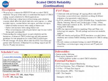
- We propose to continue the NEPP FY06 task on
scaled CMOS reliability. The goal of this task is
to understand the impact of CMOS scaling on parts
reliability for NASA applications. - CMOS technology scaling has posed increasing
parts reliability concerns which affect the whole
bath tube curve regions, i.e., infant mortality
region, constant failure rate region, and
wear-out region. - Infant mortality increases with scaling in
feature size - Failure rate increases with scaling feature size
- Wear-out mechanisms induced parts failure may
become visible during parts operating life - Understanding the scaling impact on parts
reliability and the limitations of advanced CMOS
technology will help generate guidelines for risk
mitigations for scaled CMOS technologies. - We will leverage off similar efforts with the
AVSI Consortium and partner with University of
Maryland for modeling support and 3D Plus for 3rd
party test services.
- FY07 Plans
- Collaborate with and leverage off ongoing efforts
with AVSI Consortium on microelectronics
reliability modeling lifetime evaluation of
progressively scaled devices. - In FY06, reliability testing on DDR SDRAMs from 3
manufacturers (Elpida, Samsung, Micron) and 3
technologies (110nm, 100nm, 90nm) started and
continues at JPL. In FY07, we will continue this
testing DDR SDRAMs. - AFRL has expressed interest in supplying 65nm and
90nm core technology test samples. We will
package and stress test available samples. - UMD will develop and perform SPICE simulation on
scaled device reliability and continue FaRBS
derating simulation for CMOS scaling impact. - JPL will continue accelerated testing on scaled
SDRAMs and 65nm/90nm core technologies using
in-house and 3rd party test resources.
Schedule/Costs
- Deliverables
- Interim update, Mid-year
- Final report, September 2007
- NASA guideline update on scaled CMOS reliability
- External Partners
- AVSI Consortium, Planned Membership
- Prof Joey Bernstein, Univ of Maryland - Modeling
Support - 3-D Plus 3rd Party Test Support
- Dave Alexander, AFRL Test Samples
- AMI Test Samples
Lead Center/PI JPL, Mark White Co-PI JPL, Yuan
Chen
Synergistic with Par-1.


