Phase Locked Loops - PowerPoint PPT Presentation
1 / 14
Title:
Phase Locked Loops
Description:
Carry out bit is asserted when accumulator residue reaches or surpasses its full ... Accumulator residue corresponds to instantaneous phase error ... – PowerPoint PPT presentation
Number of Views:304
Avg rating:3.0/5.0
Title: Phase Locked Loops
1
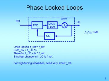
Phase Locked Loops
VCO
Ref
LO
PFD
Loop Filter
fLOfrefN/M
1/N
Once locked, f_ref f_div But f_div f_LO /
N Therefor, f_LO N f_ref. Smallest change in
f_LO is f_ref. For high tuning resolution, need
very small f_ref.
2
Conflict between freq resolution and PLL
bandwidth / settling time
- Since PFD is controlled by f_ref, hence
f_sampling f_ref - For stability and transfer characteristics, need
f_ref to be 10s of times of PLL bandwidth - Hence, f_BW 0.01 to 0.1 f_ref
- PLL settling time k 1/_BW
3
Increasing freq resolution and BW
VCO
Ref
LO
fLOfrefN/M
1/M
PFD
Loop Filter
Phase-Locked Loop
1/N
After lock, PFD input signals have the same
freq. Hence, f_ref / M f_LO / N Therefor,
f_LO f_ref N/M Freq resolution f_ref
(N1/M1 N2/M2) PFD sampling freq f_sampling
f_ref / M PLL bandwidth 0.02 to 0.05 f_ref / M
4
Phase Locked Loops
VCO
Ref
LO
PFD
Loop Filter
1/N
N
dither
N1
N N1 dither In lock, f_LO average(N)
f_ref. Smallest change in f_LO can be very fine.
5
Phase Locked Loops
VCO
Ref
LO
PFD
Loop Filter
dither
1/N
N_frac
Carry out
Accumulator
Smallest increments in N_frac sets freq
resolution. Problem periodic errors.
6
For N 4.25, user integer 4 and N_frac 0.25 In
every 4 cycles, div by 4 three times and div by 5
once
When carry signal is generated, swallow one VCO
cycle Notice the periodic error signal that feed
into fileter
7
Accumulator Operation
- Carry out bit is asserted when accumulator
residue reaches or surpasses its full scale value - Accumulator residue corresponds to instantaneous
phase error - Increments by the fractional value input into the
accumulator
8
Phase Locked Loops
VCO
Ref
LO
PFD
Loop Filter
dither
1/N
Sigma-Delta modulator
N_sd
N N or N1
Riley US Patent 4965531, 1989 JSSC 93MASH
Noise shaping. Removes periodic tones.
9
The amount of noise depends on PLL band
width. Smaller BW ? lower noise
10
Divider
- At high frequency, divider block is challenging
to design - It consumes a lot of power
- Typically implemented using several stages
- Can have each stage operating at gradually lower
freq to save power
11
Divide-by-2 Circuit
- Achieves frequency division by clocking two
latches (i.e., a register) in negative feedback - Latches may be implemented in various ways
according to speed/power requirements
12
- Advantages
- Reasonably fast, compact size
- No static power dissipation, differential clock
not required - Disadvantages
- Slowed down by stacked PMOS, signals goes through
three gates per cycle - Requires full swing input clock signal
13
- Very fast due to small swing and absence of PMOS
devices - Additional speedup can be obtained by using
inductors - High power, large area
- Differential signals required, Biasing sources
required
14
Divide by 2 or 3
- Normal mode of operation CON 0 ?Y 0
- Register B acts as divide-by-2 circuit
- Divide-by-3 operation CON 1 ?Y 1
- RegB remains high for an extra cycle
- Causes Y to be set back to 0 ?RegB toggles again
- CON must be set back to 0 before RegB toggles to
prevent extra pulses from being swallowed


