ADC and TDC Implemented Using FPGA PowerPoint PPT Presentation
1 / 1
Title: ADC and TDC Implemented Using FPGA
1
ADC and TDC Implemented Using FPGA
Jinyuan Wu, S. Hansen and Z. Shi Fermi National
Accelerator Laboratory, Batavia, IL 60510, USA
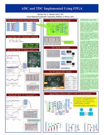
FPGA ADC and TDC Intrinsically, FPGA is a
digital device. However, with suitable use of
the FPGA resources, it is possible to use FPGA to
digitize multi-channel analog waveforms. The
digitized waveforms can be directly processes in
the FPGA. There are several possible schemes of
digitizing analog signals. One of the schemes we
used in our FPGA ADC study is based on the
ramping-comparing approach. In todays FPGA
devices, differential input buffers are good
comparators within a sufficiently large range of
input voltage levels, since they are designed to
be compatible with various differential signaling
standards. Comparator-based ADC schemes can be
implemented with FPGA. In our tests, the analog
inputs are directly connected to the FPGA input
pins. A passive RC network is connected to the
FPGA output pins so that a periodic reference
voltage ramp can be generated. The differential
input buffers are used as comparators to generate
logic transitions inside the FPGA when the
reference voltage ramps across the input voltage
levels. The transition times are digitized by the
TDC block implemented in the FPGA. Since the
period, the RC network parameters and the
starting time of the ramps are known the input
voltage levels can be derived from the transition
times. (In some references, the single-slope
scheme is mistakenly referred as Wilkinson ADC
that is based on dual-slope principle.) A key
functional block, Time-to-Digit-Converter (TDC)
is needed in FPGA. The TDC we used in this work
is multi-sampling scheme with quad clock. In our
TDC design, the four samples are transferred into
a bit pattern in a single clock domain
immediately and only one set of edge detect,
pulse filter and count latch circuit is used.
The meta-stability is limited at the sampling
stage only and in fact, the meta-stability in
sampling stage does no harm but carrying the
input signal arrival time information. The
decoding becomes very simple in our design. The
detail is described in the paper. The TDC in
FPGA alone is already very useful. The TDC card
designed for Fermilab MIPP upgrade project is
documented in this paper. The multi-sampling
structure can have other applications. A
deserializer circuit known as Digital Phase
Follower (DPF) is also documented. Using DPF,
any FPGA input can be used to receive serial data
without needing dedicated deserializer that is
only available in high-end FPGA families. The
DPF can compensate input data phase drift not
only due to cable temperature variation, but also
due to crystal oscillator frequency difference
between transmitter and receiver.
FPGA Direct Analog Signal Digitization
Multi-Sampling Based TDC
Single Slope ADC Ramping-Comparing
Internal Layout Inside FPGA
Single Slope ADC ! Wilkinson ADC
TDC Bench Test Results
Test Result BD3_19, Quasi-Linear VREF
The 96-Channel TDC Module
48CH TDC FPGA
48CH TDC FPGA
Data Concentration FPGA
Digital Phase Follower (DPF) A TDC-Like
Deserializer
Test Result BD4_22, Exponential VREF
- It is used for serial communication between
low-cost FPGA devices. - No dedicated clock-data-recovery (CDR) circuitry
is needed. - It tolerates multi-crystal operations.
The data measured by trailing ramp is much more
smoother than the leading ramp for small pulses.

