Wafer - PowerPoint PPT Presentation
Title:
Wafer
Description:
Andrew B. Kahng1, Ion Mandoiu2, Xu Xu1, and Alex Z. Zelikovsky3 1. CSE Dept. University of California, San Diego 2. CSE Departments, University of Connecticut – PowerPoint PPT presentation
Number of Views:34
Avg rating:3.0/5.0
Title: Wafer
1
Yield-Driven Multi-Project Reticle Design and
Wafer Dicing Andrew B. Kahng1, Ion Mandoiu2, Xu
Xu1, and Alex Z. Zelikovsky3 1. CSE Dept.
University of California, San Diego 2. CSE
Departments, University of Connecticut 3. CS
Department, Georgia State University
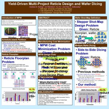
ABSTRACT
Introduction of MPW
Wafer Shot-Map Definition
- Mask cost is predicted to be over 1M for 90 nm
- Wafer cost is around 4K
- Multi-Project Wafer share costs of mask tooling
between multiple - prototype and low production volume designs
The aggressive scaling of VLSI feature size and
the pervasive use of advanced reticle enhancement
technologies has lead to dramatic increases in
mask costs. Multiple project wafers (MPW), or
shuttle runs, provide an attractive solution
for such low volume designs, by providing a
mechanism to share the cost of mask tooling among
up to tens of designs. However, MPW reticle
design and wafer dicing introduce complexities
not encountered in typical, single-project
wafers. In this work we propose a general MPW
flow including four main steps (1)
schedule-aware project partitioning, (2)
multi-project reticle floorplanning, (3) wafer
shot-map definition, and (4) wafer dicing plan
definition. Experiments on industry testcases
show that our methods significantly outperform
not only previous methods in the literature, but
also reticle floorplans manually designed by
experienced engineers.
- Stepper Shot-Map Design Problem
- Given Reticle floorplan, wafer diameter
- Find Wafer center location
- To minimize Wafer cost
- Our method Grid-based Shot-Map Design
- achieves 13.6 wafer cost reduction
Project
Wafer
Reticle
Schedule-aware Partition
Reticle image
Manufacturing Cost Minimization
Wafer shotmap
- Delay cost cannot be ignored in practice
- Project Partitioning Problem
- Given reticle size, a set of projects
- Find a partition of projects into reticles
- To minimize sum of mask cost and delay cost
- Our method Schedule-aware partitioning leads to
- 72.6 cost reduction vs. schedule-blind
partitioning
- MPW Cost Minimization Problem
- Given Projects to be manufactured,
- wafer diameter and reticle size
- Find Reticle and wafer design, dicing lines
- To minimize Manufacturing cost
Multiple Wafer Dicing
- Side-to-Side Dicing Problem
- Given Reticle floorplan,
- Wafer shot-map
- Find Dicing lines
- To minimize Wafer cost
Reticle Floorplan
MPW Design Flow
- Reticle Floorplan Problem
- Given a set of projects and reticle size
- Find placement of projects within the
reticle - and dicing lines
- To Minimize the number of wafers used
- Key challenge wafer cost calculation /
estimation - Greedy Dicing Simulated Annealing (ISPD
2004) - Grid-packing Branch and Bound (ICCD 2004)
- Our method Hierarchical Quadrisection Floorplan
Projects and Parameters
Project Partition
Reticle Floorplan
Stepper Shotmap
- Previous methods
- Single Wafer Multiple Row-Column (SWMRC)
- Wafers use the same dicing lines, rows
(columns) of - each wafer use different lines
- Multiple Wafer Single Row-Column (MWSRC)
- Wafers use different dicing lines, rows
(columns) of - each wafer use the same lines
- Our method
- Multi-Wafer Multiple Row-Column (MWMRC)
- Wafers use different dicing lines, rows
(columns) of - each wafer use different lines
Dicing Plan Definition
CONCLUSIONS
- Improved algorithms for MPW design flow
- Schedule-aware partitioning 72.6 cost
reduction - HQ reticle floorplan 16.1 wafer cost reduction
- Wafer shot-map definition 13.6 cost reduction
- Multiple wafer dicing 42.1 wafer cost
reduction - Future work Multi-layer reticle design
16.1 reduction
42.1 reduction
BIBLIOGRAPHY
- Kahng et al., Multi-Project Reticle
Floorplanning and Wafer - Dicing, ISPD 2004
- Kahng et al., Reticle Floorplanning With
Guaranteed Yield for - Multi-Project Wafers, ICCD 2004
- Xu et al. A Multi-objective Floorplanner for
Shuttle Mask - Optimization, BACUS 2004
- Xu et al. CMP Aware Shuttle Mask Floorplanning
, - ASPDAC 2005


