
Semiconductor Metallization PowerPoint PPT Presentations
All Time
Recommended

DESIGN FOR SEMICONDUCTOR RELIABILITY George Denes, Dipl.Eng. Senior Semiconductor Reliability Consultant SEMICONDUCTOR DEVICE LIFE STAGES To evaluate the reliability ...
| PowerPoint PPT presentation | free to view

The attached narrated power point presentation attempts to explore the construction and working of different types of semiconductor materials.
| PowerPoint PPT presentation | free to download

Semiconductors At zero temperature semiconductors are insulators with completely filled bands. At higher temperatures they conduct at due to the thermal excitation of ...
| PowerPoint PPT presentation | free to view

This process is known as ... a/3 etc are those critical values - like waves resonating on ... Place EF midway between donor state and conduction band. 41. Fermi ...
| PowerPoint PPT presentation | free to view

at the top of the valance band. for excitation. Unity in denominator can be ignored ... and electron) and acceptor level is close to the valance band ...
| PowerPoint PPT presentation | free to view

To excite electrons from valence band to conduction band, extra energy is needed: ... and the electrons, and the easier to excite an electron into the conduction band ...
| PowerPoint PPT presentation | free to view

In semiconductors, we think of positive charges (holes) and negative charges ... Most practical semiconductors rely on impurities for their properties ...
| PowerPoint PPT presentation | free to view

P-n junction diode and other semiconductor
| PowerPoint PPT presentation | free to download
An introduction to semiconductor detector physics as applied to particle physics ... 4 lectures can't cover much of a huge field. Introduction. Fundamentals ...
| PowerPoint PPT presentation | free to download

(Ga,Mn)As and its simple picture (Ga,Mn)As in reality. band ... anneal them away ! One can anneal away ! Annealing [Potashnik et al. APL 79, 1495 (2001) ...
| PowerPoint PPT presentation | free to view

Llobregat Abell n, Alejandra Arribas Jaen, Elisabeth ESTRUCTURA DE BANDAS DE ENERG A DE LOS S LIDOS ESTRUCTURA CRISTALINA DE LOS SEMICONDUCTORES SEMICONDUCTORES ...
| PowerPoint PPT presentation | free to view

Imagine a world without chips: no smartphones, no laptops, no digital cameras. That is why shaping performs a critical function in semiconductor manufacturing. The rolled rings manufacturer uses precision and difficult forgings to create additives that are essential for digital devices to work effectively.
| PowerPoint PPT presentation | free to download

Semiconductor Lasers Aashwinder Lubana Brian Urbanczyk Harpaul Singh Kumar Kunal Chopra Introduction Light Amplification by Stimulated Emission of Radiation.
| PowerPoint PPT presentation | free to download

Semiconductors and Diodes Bands, gaps, etc.
| PowerPoint PPT presentation | free to download

Electronics Tutorial (Thanks to Alex Pounds) Electronics Tutorial ... Testing via ohm meter. Two diodes back to back: test each separately for impedance ratio ...
| PowerPoint PPT presentation | free to view
9. Semiconductors Optics Absorption and gain in semiconductors Principle of semiconductor lasers (diode lasers) Low dimensional materials: Quantum wells, wires and dots
| PowerPoint PPT presentation | free to download
26.8: Semiconductors: Pure silicon has a high resistivity and it is effectively an insulator. However, its resistivity can be greatly reduced in a controlled way by ...
| PowerPoint PPT presentation | free to download

makes up about 28% of earth's crust and is 2nd most abundant element ... Silicon/plastic fluidic coupler to standard capillary tubing. ...
| PowerPoint PPT presentation | free to view

An Integrated Circuit is generally expressed in the form of a chip. Made in one unit, it’s an electrical parts assembly. However, a wafer represents small slices of silicon. In the production of integrated circuits like the integrated circuits are used in most semiconductor wafers, these are utilized.
| PowerPoint PPT presentation | free to download

seguindo o link em 'Semin rios, Mini-cursos, etc. ... hysteresis FM with easy axis in plane; remanence vs. T Tc ~ 60 K. x = 0.035. x = 0.053 ...
| PowerPoint PPT presentation | free to view
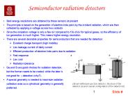
Best energy resolutions are obtained by these sensors at present The principle is based on the generation of electron-hole pairs by the incident radiation, which are ...
| PowerPoint PPT presentation | free to download

Metallization1. 1. Metallization (Jaeger Chapter 6 Campbell Chapter 12) Contact to the different regions of the semiconductor forming a device and ...
| PowerPoint PPT presentation | free to download

Valence Band. Overlapping bands - little energy is needed for conduction. Conductor ... Silicon atoms share valence electrons to form insulator-like bonds. ...
| PowerPoint PPT presentation | free to view

* INTRODUCTION Spintronic devices manipulate current with charge and spin This added degree of control will require ... Ferromagnetism in Mn doped group IV ...
| PowerPoint PPT presentation | free to download

... Web Page: from http://www.novellus.com/damascus/boc/boc.htm ... Rajeev Bajaj,.' Copper CMT challenges,' Semiconductor International, June 1998, pp. 91-96. ...
| PowerPoint PPT presentation | free to view

Lecture 1 Introduction to Semiconductor Semiconductor Semiconductors are materials with conductivity that can be controlled through methods such as doping or changing ...
| PowerPoint PPT presentation | free to view

Compound Semiconductor Market report categorizes global market by Type (III-V, II-VI, IV-IV, Sapphire), Deposition Technology (CVD, MBE, HVPE, Ammonothermal, MOVPE, LPE, ALD), Product (Power, Opto - Electronic), Application, and Geography.
| PowerPoint PPT presentation | free to download
Agreement to Acquire Digital Broadcast Technology Assets, Expertise from Zarlink ... motion-detecting sensors that could help senior citizens live more independently. ...
| PowerPoint PPT presentation | free to download

This barrier simulates the behavior of a pn-junction. Recovery charge of this diode is much less than the equivalent pn-junction diode. ...
| PowerPoint PPT presentation | free to view

Many free electrons not tied up in chemical bonds. Insulators. All electrons (in intrinsic material) tied up in chemical bonds ...
| PowerPoint PPT presentation | free to download

SOLIDS AND SEMICONDUCTOR DEVICES - I Energy Bands in Solids Energy Band Diagram Metals, Semiconductors and Insulators Intrinsic Semiconductor Electrons and Holes
| PowerPoint PPT presentation | free to view

states that are free to move through the material. Insulators always have virtually zero electrons in such ... all the electrons are stuck in valance bands ...
| PowerPoint PPT presentation | free to download

Title: PowerPoint Presentation Author: Pugliese, William Last modified by: pokie Created Date: 1/1/1601 12:00:00 AM Document presentation format: On-screen Show
| PowerPoint PPT presentation | free to view

Modern wafers are 8-12' in diameter, and only a few millimeters deep. ... http://www.eet.com/news/latest/showArticle.jhtml?articleID=177105678&pgno=1 ...
| PowerPoint PPT presentation | free to view
Huge number of transistors can be integrated in a small Si chip. ... Integration in 7000 times in 25 years, (Moor's Law) Clock Speed : 700 times in 25 years ...
| PowerPoint PPT presentation | free to download
states that are free to move through the material. Insulators always have virtually zero ... CMOS Inverters (a) CMOS inverter structure. ( b) Transition curves. ...
| PowerPoint PPT presentation | free to download

Title: SEM CONDUCTOR DEV CE PHYS CS Author: halil Last modified by: cloti Created Date: 4/3/2005 1:51:06 PM Document presentation format: Presentaci n en pantalla
| PowerPoint PPT presentation | free to download

Raytheon. 5. Current Flow In Semiconductor ... Raytheon. 6. Diode. RF switching can be performed using high performance P-I-N diodes: ...
| PowerPoint PPT presentation | free to view

Applications in Nuclear and Particle Physics. Accelerators and ... the structure is called zinc blende, example III-V semiconductors include GaAs and AlAs. ...
| PowerPoint PPT presentation | free to view
Close packed/herringbone arrangement. 2.21 eV room temp band gap ... Close packed/herringbone arrangement. Rigid Rod with 1 deviation from a plane ~2.2 eV band gap ...
| PowerPoint PPT presentation | free to download

Semiconductor Devices and Physics (Ch. 1) Why semiconductor? Foundation of the electronic industry Including applied physics, electrical engineering, electronics ...
| PowerPoint PPT presentation | free to view

This added degree of control will require materials that have magnetic ... or nuclear and electron spins throught the hyperfine interaction within MF theory ...
| PowerPoint PPT presentation | free to view
Metal-semiconductor (MS) junctions Many of the properties of pn junctions can be realized by forming an appropriate metal-semiconductor rectifying contact (Schottky ...
| PowerPoint PPT presentation | free to download

Metal-Oxide-Semiconductor (MOS) EBB424E Dr. Sabar D. Hutagalung School of Materials & Mineral Resources Engineering, Universiti Sains Malaysia MOS (Metal-Oxide ...
| PowerPoint PPT presentation | free to view

The Semiconductor Equipment Austin Company is also one of the distributors of a well-known product type called the Ultrasonic Cleaning Machines. These machines use ultrasound technology to clean delicate surfaces. #SemiconductorEquipmentAustin
| PowerPoint PPT presentation | free to view

Title: SEMICONDUCTORES Y CIRCUITOS INTEGRADOS Author: Inversiones Vargas Arana Last modified by: JIMY ALEXANDER ROMERO MORENO Created Date: 5/7/2004 1:50:05 PM
| PowerPoint PPT presentation | free to view

Semiconductors are materials that conduct electricity better than insulators like ceramics, but not as well as conductors like metals. They can be compounds like gallium arsenide or pure elements like germanium or silicon. The function of semiconductor is to control and manage the flow of electric current in electronic equipment and devices. From smartphones to home appliances, cars, transportation, and medical devices, semiconductors power almost all the technology that we rely on today
| PowerPoint PPT presentation | free to download

Global semiconductor wafer cleaning equipment market is set to witness a substantial CAGR of 6.95% in the forecast period of 2019- 2026
| PowerPoint PPT presentation | free to download

Aarkstore Enterprise culminates the newest Market Research Report "Taiwanese Semiconductor Manufacturing Industry, 4Q 2018"
| PowerPoint PPT presentation | free to download

Si -- diamond lattice structure a = 5.4Angstrom. Face-centred cubic lattice. ... Occupied conduction and valance-band states: Modification of carrier density and ...
| PowerPoint PPT presentation | free to view

Chapter 2-1. Semiconductor models ... Both bond model and band model shows us that semiconductors behave like insulators at 0K. ...
| PowerPoint PPT presentation | free to view
Reduction of gate length (lithography) Increase of impurity concentrations ... Lithography. EUV prototype. NIKHEF, July 4, 2003. Jurriaan Schmitz, University of Twente ...
| PowerPoint PPT presentation | free to download

Semiconductor Memory Design (SRAM & DRAM) Kaushik Saha Contact: kaushik.saha@st.com, mobile-98110-64398 Understanding the Memory Trade The memory market is the most ...
| PowerPoint PPT presentation | free to view

Energy Band View of Semiconductors Conductors, semiconductors, insulators: Why is it that when individual atoms get close together to form a solid such as copper ...
| PowerPoint PPT presentation | free to download

EEL Chip size: 500 x 500 x 100 um3. 8/22/09. Chang-Hasnain. 5. p-DBR. n-DBR. gain medium ... Fabry-Perot EEL vs. VCSEL. Gain. Free Spectral Range. 500 mm ~2mm ...
| PowerPoint PPT presentation | free to view
large & persistent el. fields. transistors, logic, sensitive to doping and ... MRAM universal memory. fast, small, low-power, durable, and non-volatile ...
| PowerPoint PPT presentation | free to download