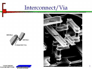
Interconnect/Via - PowerPoint PPT Presentation
Title:
Interconnect/Via
Description:
Title: Slide Title Author: Dhamin Al-Khalili Description: Some of the material has been copied from Rabaey/Prentice Hall Last modified by: Asim Al-Khalili – PowerPoint PPT presentation
Number of Views:85
Avg rating:3.0/5.0
Title: Interconnect/Via
1
Interconnect/Via
2
Delay of Devices and Interconnect
3
Reduction of the feature size
The difference in the arrival times of the clock
signal to all registers in a synchronous digital
system
4
An Example , The Clock Distribution Network
(CDN)
A set of interconnections that delivers reliably
a time reference, clock signal , to every
register element in a synchronous digital system.
PowerPC microprocessor 32,000 master/slave latch
5
Power Consumption Routing and system complexity
P CV2f
6
Delay model of the CDN, Elmore Delay model
It takes into account the interconnect resistance
and capacitance and the capacitance of the
registers
7
Example Routing delay problems The Clock
Skew
The difference between time arrivals of the clock
signal to all the registers in a synchronous
digital system
S(ij) Ti - Tj
Two conditions
8
Minimizing the effects of delay, The H_Tree
If it is possible to divide the set of registers
R into two symmetric sets recursively and
alternatively by vertical and horizontal lines,
then the set R can be connected by an H-tree
9
Interconnect Length
10
Interconnect/Via
11
Cross Section View of Capacitances in interconnect
Units are in Angstrom, 1A0.1nm
12
Interconnect
Interconnects in chips are routed in several
layers horizontally and vertically and used
according to their application
13
Parallel and fringing Capacitance
14
Fringing Capacitance
T is the thickness of wire H is the distance of
wire to substrate.
15
Cross Talk
16
Fringing/ Parallel Plate Capacitance of
Interconnect
17
Modeling Interconnect
LUMPED MODEL
T-MODEL
-MODEL
2T-MODEL
2p -MODEL
18
Modeling of Interconnect
19
Delay of Interconnect
Capacitance C/unit area L (length) W
(width) C
Resistance R/ number of squares R
20
Delay comparison
21
Example
A signal is propagated on a 6mm length metal 1
(M1) interconnect of CMOSIS5 Process, using
minimum wire width. Calculate the delay and
comment on methods for reducing this delay.
22
Different Path
23
Thank you !
24
What is the maximum size of silicon chip?
- Power dissipation
- Packaging
- Number of pins
- Technology
- The interconnect
- used
25
Inductances
For die wires
h is the height of the wire above the
substrate, d is the diameter of the wire is
the magnetic permeability of the material
26
Inductance
For on-chip,
h is the height of the wire above the
substrate, d is the diameter of the wire is
the magnetic permeability of the material
27
Example on VDD Bounce
Determine the values of due to
inductive and resistive losses when the output
driver sources 10mA in 1.5ns in the following
circuit.
28
Example on Power lines
What will be the power line width if you drive a
10pF load at 1GHz Assume Vdd3.5V.
29
Example on Charge Sharing
Calculate the drop in voltage for 64 read lines
each consisting of 0.1pF capacitances. Assume
bus capacitance to be 10pF.
30
Thank you !


